Luminescence conversion of led

Active Publication Date: 2009-11-12
OSRAM OLED
View PDF17 Cites 5 Cited by
  • Summary
  • Abstract
  • Description
  • Claims
  • Application Information

AI Technical Summary

Benefits of technology

[0010]By contrast, the process according to the invention allows the production of highly efficient LEDs with very good color rendering which also have a particularly homogenous radiation emission characteristic.
[0011]The process according to the invention consists in applying a thin near-chip film, preferably with a thickness of at most 40 μm, in particular 10 to 40 μm, of a red phosphor (known as chip-level coating/on-chip coating) direct to the chip which emits with a short wavelength and may in particular have a peak wavelength in the range from 300 to 400 nm, i.e. in the UV to preferably blue radiation region, it being possible for the film to be applied, for example, by means of screen printing or electrophoresis. Various suitable methods are described in more detail in U.S. Pat. No. 6,686,691. This chip which has been coated in this way is either potted directly with potting resin containing converter or is introdu

Problems solved by technology

This absorption process also has an adverse effect on the efficiency of the LED, since the absorbed light is not completely converted into red luminescent light.
The generally undesirable shift in the green or yellow emission usually result

Method used


Image

  • Luminescence conversion of led
  • Luminescence conversion of led
  • Luminescence conversion of led

Examples


Example

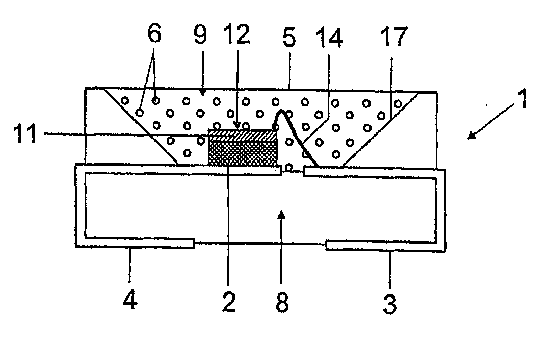
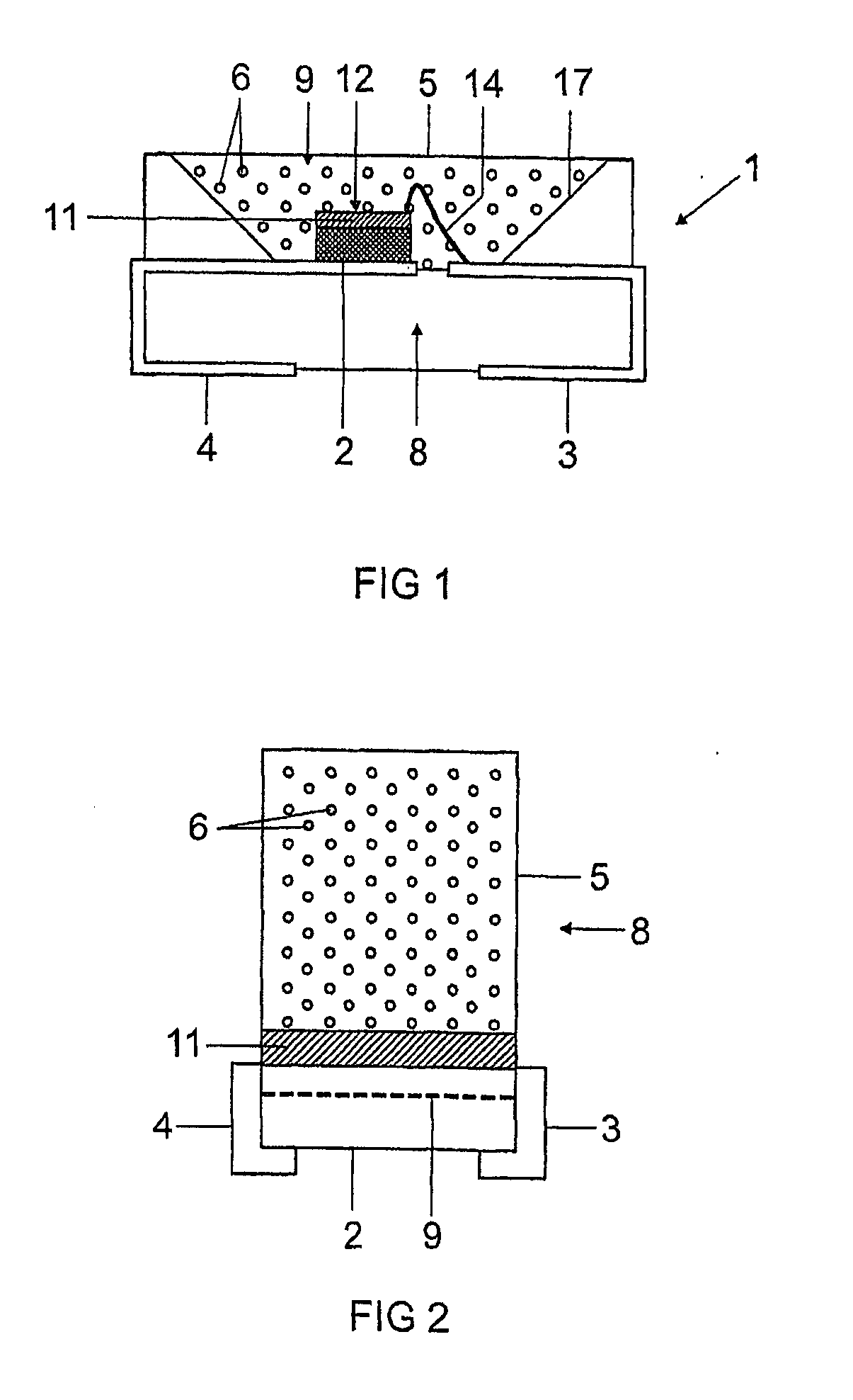
[0018]By way of example, a structure which is fundamentally similar to that described in U.S. Pat. No. 5,998,925 is used for a white LED together with an InGaN chip. The structure of a light source of this type for white light is specifically shown in FIG. 1. The light source is a semiconductor component 1 having a chip 2 of the InGaN type with a peak emission wavelength of 460 nm, i.e. in the blue, with first and second electrical terminals 3, 4, embedded in an opaque basic housing 8 in the region of a recess 9. One of the terminals 3 is connected to the chip 2 via a bonding wire 14. The recess has a wall 17 which serves as reflector for the blue primary radiation of the chip 2. The red phosphor is applied direct to the chip in the form of a thin film 11. This red phosphor is preferably a nitridosilicate of the MxSiyNz:Eu type, where M=Ca, Sr, Ba, Zn. In this context, it is preferable that z=2 / 3x+4 / 3y. This phosphor is known per se, for example from EP 1 153 101 (Eu-red LED).

[0019]...


PUM


Abstract

A luminescence conversion of LED, which uses a blue emitting chip and two illuminating substances, whereby one emits a red and the other a yellow to green. Both illuminating substances are separated upstream from the chip.

Description

FIELD OF THE INVENTION[0001]The invention is based on a luminescence conversion LED as described in the preamble of claim 1. It deals in particular with an LED with a high conversion efficiency.BACKGROUND OF THE INVENTION[0002]U.S. Pat. No. 6,686,691 has disclosed a luminescence conversion LED, in which the primary light source used is a blue chip. A phosphor layer containing two phosphors, which absorb blue and emit green and red, is connected ahead of the chip. In this case, however, the two phosphors are distributed homogenously in the resin, which leads to undesirable effects. It is accordingly not possible to satisfy the two criteria of “high efficiency” and “good color rendering” simultaneously. To achieve a high color rendering, either a green phosphor which actually has too short a wavelength has to be used, with this then being shifted by the strong absorption of the red phosphor, or the red phosphor has to be shifted as far as possible toward a long wavelength. Both soluti...

Claims


Application Information

Patent Timeline
IPC IPC(8): H01L33/00H01L33/50
CPCH01L33/504H01L2224/48091H01L2924/00014
Inventor BRAUNE, BERTJERMANN, FRANKSTRAUSS, JORG
Owner OSRAM OLED
Why Eureka
Try Eureka