Dynamic alignment of wafers using compensation values obtained through a series of wafer movements

a compensation value and wafer technology, applied in the field of transfer wafers, can solve problems such as imperfect sensors, inaccurate wafer position calculation, and poor accuracy of placement wafers, and achieve the effect of accurate fine tuning values

Active Publication Date: 2009-11-12
LAM RES CORP
View PDF56 Cites 36 Cited by
  • Summary
  • Abstract
  • Description
  • Claims
  • Application Information

AI Technical Summary

Benefits of technology

[0018]8. fine tune offset table values and robot position for each station by obtaining data from repeatedly placing and picking of the wafer. By using multiple measures and generating a representative value, the system is able to obtain more accurate fine tuning values.

Problems solved by technology

However, the accuracy for placing wafers suffers due to multiple factors.
For example, the position of the sensors may not be perfect and small deviations in sensor location result in defects when calculating wafer position.
In addition, the robot transporting the wafer may not be in the exact place where the system believes that the robot is, which creates another source for errors.
In practice, there are operational differences between using one robot arm or the other, producing different results according to which robot arm picks up, or places the wafer when transporting the wafer.
Additionally, existing methods are susceptible to operator's errors and are not automated, requiring long calibration times.

Method used


Image

  • Dynamic alignment of wafers using compensation values obtained through a series of wafer movements
  • Dynamic alignment of wafers using compensation values obtained through a series of wafer movements
  • Dynamic alignment of wafers using compensation values obtained through a series of wafer movements

Examples


Embodiment Construction

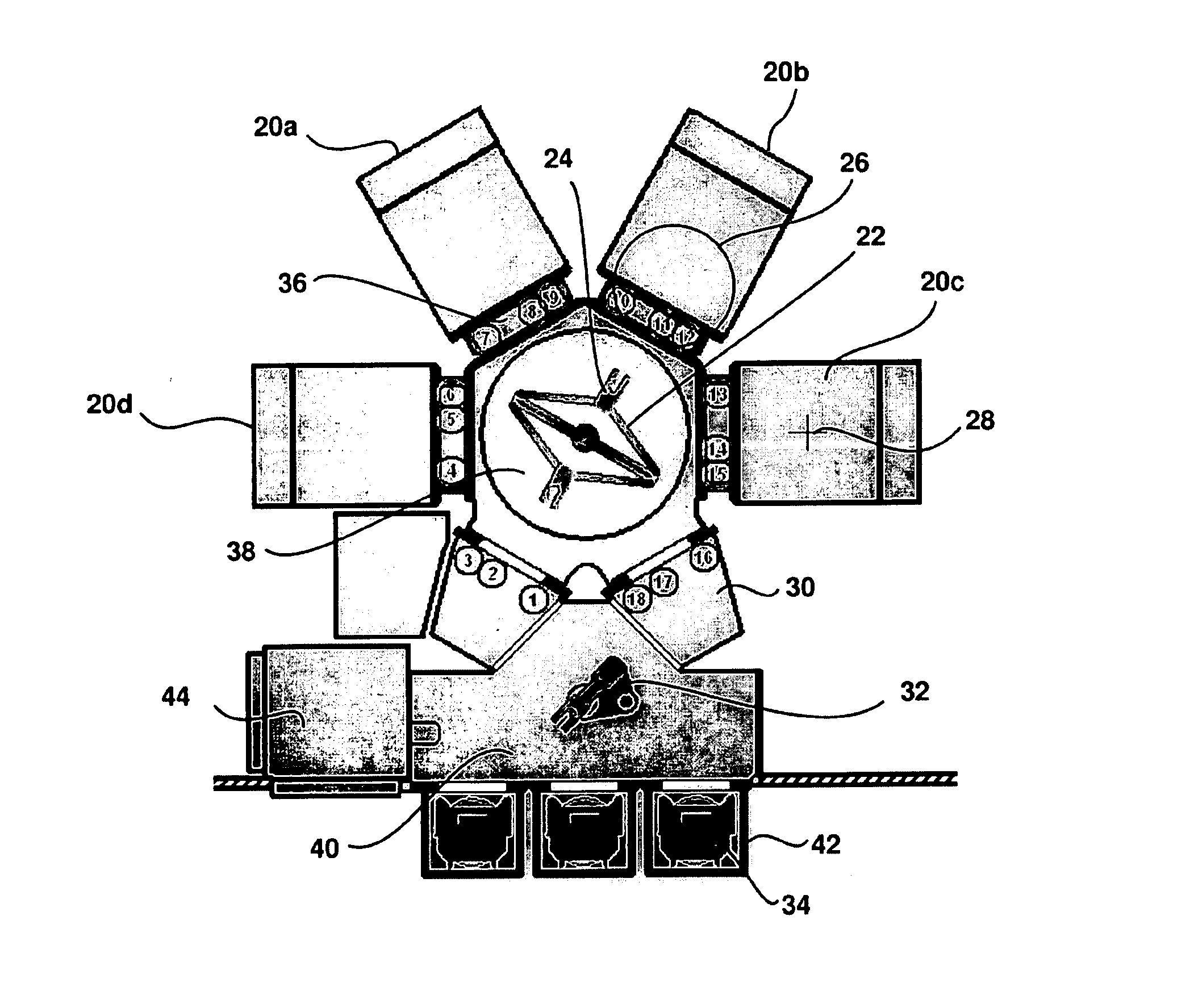
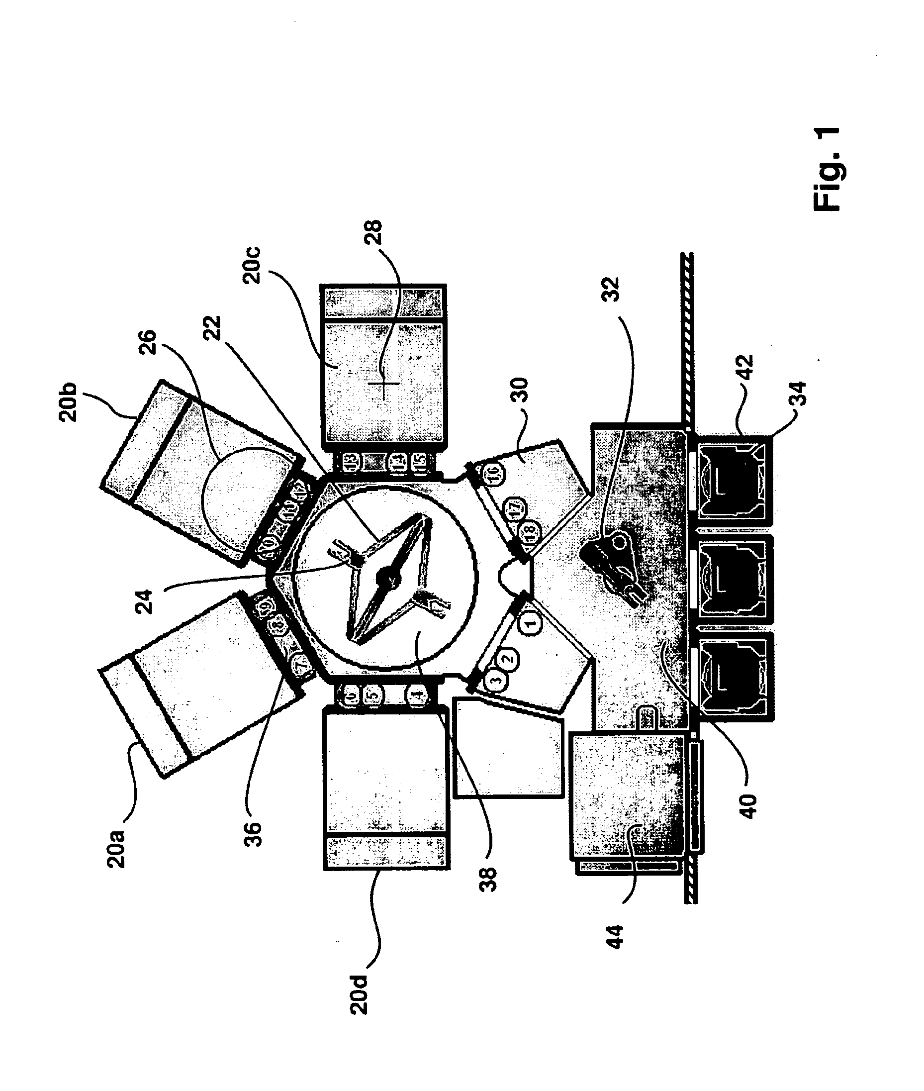
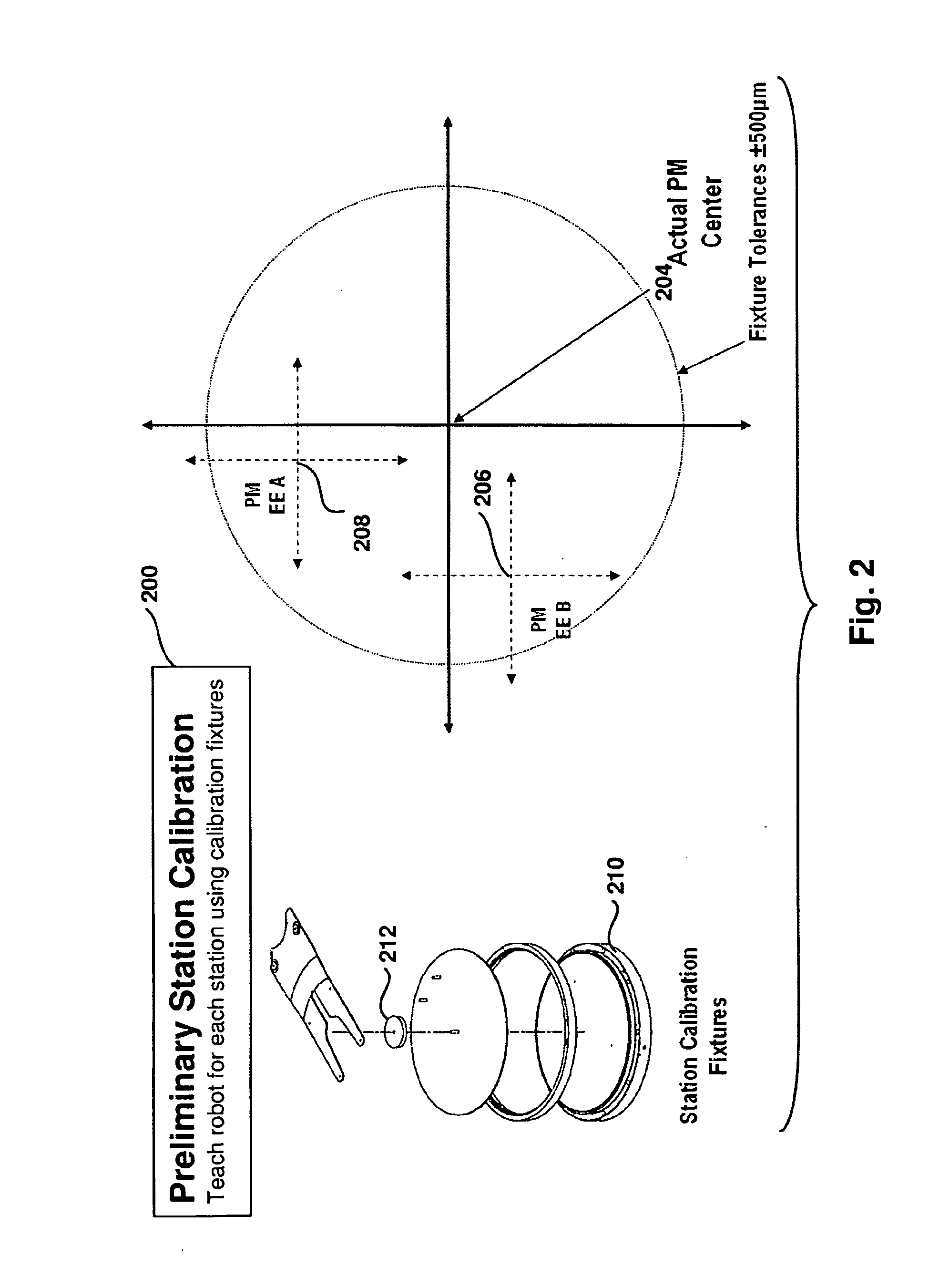
[0033]Methods and systems to optimize wafer placement repeatability in semiconductor manufacturing equipment using a controlled series of wafer movements are provided. In one embodiment, a preliminary station calibration is performed to teach a robot position for each station interfaced to facets of a vacuum transfer module (VTM) used in semiconductor manufacturing. The method also calibrates the system to obtain compensation parameters that take into account the station where the wafer is to be placed, position of sensors in each facet, and offsets derived from performing extend and retract operations of a robot arm. A well aligned wafer is used to fine tune the positioning of the wafer in each station and to help compensate for small deviations of the sensor locations from the desired location.

[0034]In another embodiment where the robot includes two arms, the method calibrates the system to compensate for differences resulting from using one arm or the other. During manufacturing,...


PUM


Abstract

Methods and systems to optimize wafer placement repeatability in semiconductor manufacturing equipment using a controlled series of wafer movements are provided. In one embodiment, a preliminary station calibration is performed to teach a robot position for each station interfaced to facets of a vacuum transfer module used in semiconductor manufacturing. The method also calibrates the system to obtain compensation parameters that take into account the station where the wafer is to be placed, position of sensors in each facet, and offsets derived from performing extend and retract operations of a robot arm. In another embodiment where the robot includes two arms, the method calibrates the system to compensate for differences derived from using one arm or the other. During manufacturing, the wafers are placed in the different stations using the compensation parameters.

Description

BACKGROUND[0001]1. Field of the Invention[0002]The present invention relates to transferring wafers among modules of semiconductor processing equipment, and more particularly to placing accurately each wafer, with the support blade that carries the wafer, inside the modules.[0003]2. Description of the Related Art[0004]In the manufacture of semiconductor devices, process chambers are interfaced to permit transfer of wafers or substrates, for example, between the interfaced chambers. Such transfer is via transfer modules that move the wafers, for example, through slots or ports that are provided in the adjacent walls of the interfaced chambers. Transfer modules are generally used in conjunction with a variety of wafer processing modules (PM), which may include semiconductor etching systems, material deposition systems, and flat panel display etching systems.[0005]A vacuum transfer module (VTM) may be physically located between one or more clean room storage facilities where wafers are...

Claims


Application Information

Patent Timeline
Patent Type & Authority Applications(United States)
IPC IPC(8): H01L21/67
CPCH01L21/68H01L21/67739
Inventor WONG, SCOTTLIN, JEFFREYBAILEY, III, ANDREW D.CHEN, JACKMOORING, BENJAMIN W.HUANG, CHUNG HO
Owner LAM RES CORP
Why Eureka
Try Eureka