Process for assembling wafers by means of molecular adhesion

a technology of molecular adhesion and wafers, which is applied in the direction of semiconductor devices, solid-state devices, radio frequency controlled devices, etc., can solve the problems of reducing the quality and value affecting the quality of multi-layer semiconductor wafers, and difficult, if not impossible, to form additional microcomponents. achieve the effect of high-quality multi-layer

Inactive Publication Date: 2009-11-12
S O I TEC SILICON ON INSULATOR THECHNOLOGIES
View PDF4 Cites 27 Cited by
  • Summary
  • Abstract
  • Description
  • Claims
  • Application Information

AI Technical Summary

Benefits of technology

[0021]The use of the assembly process of this invention allows, when transferring a layer of microcomponents, the elimination or minimization of the misalignment phenomenon (“overlay”) and permits the production of high quality multilayer s...

Problems solved by technology

However, applicant has found that after the transfer, there are cases where it is very difficult, if not impossible, to form additional microcomponents in alignment with microcomponents formed before the transfer.
These misalignments are due to heterogeneous distortions which appear in the layer coming from the initial substrate during its assembly with the final substrate.
The distortions r...

Method used


Image

  • Process for assembling wafers by means of molecular adhesion
  • Process for assembling wafers by means of molecular adhesion
  • Process for assembling wafers by means of molecular adhesion

Examples


Embodiment Construction

[0029]Reference will now be made in detail to the present preferred embodiments of the invention. The method and corresponding steps of the invention will be described in conjunction with the detailed description of the system and product obtained.

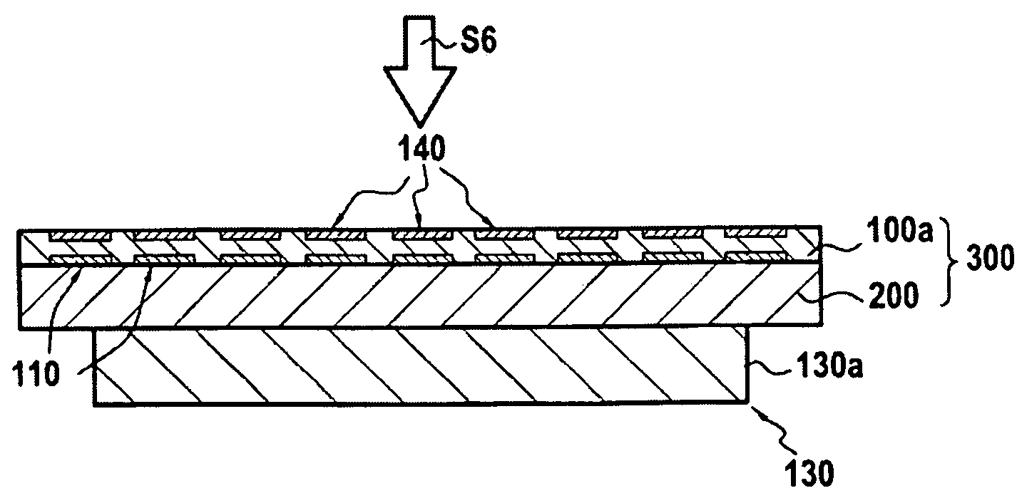
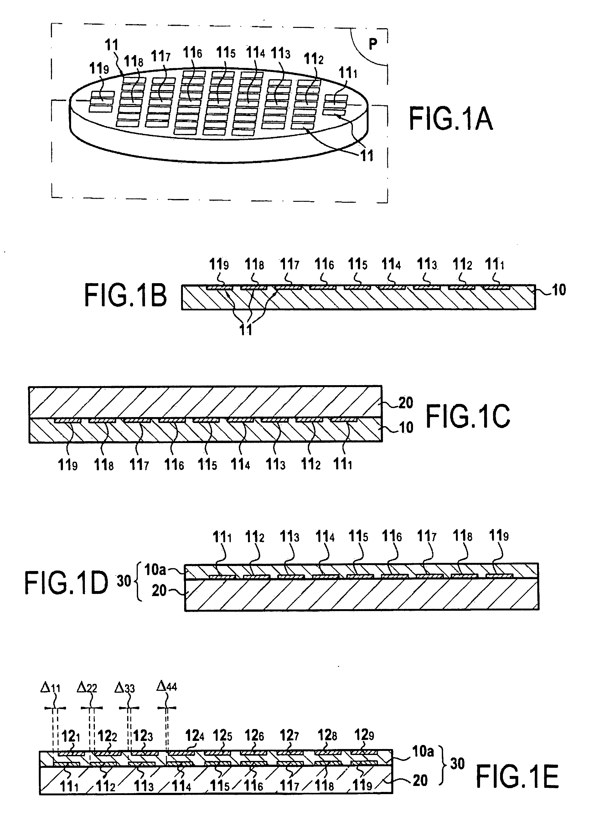
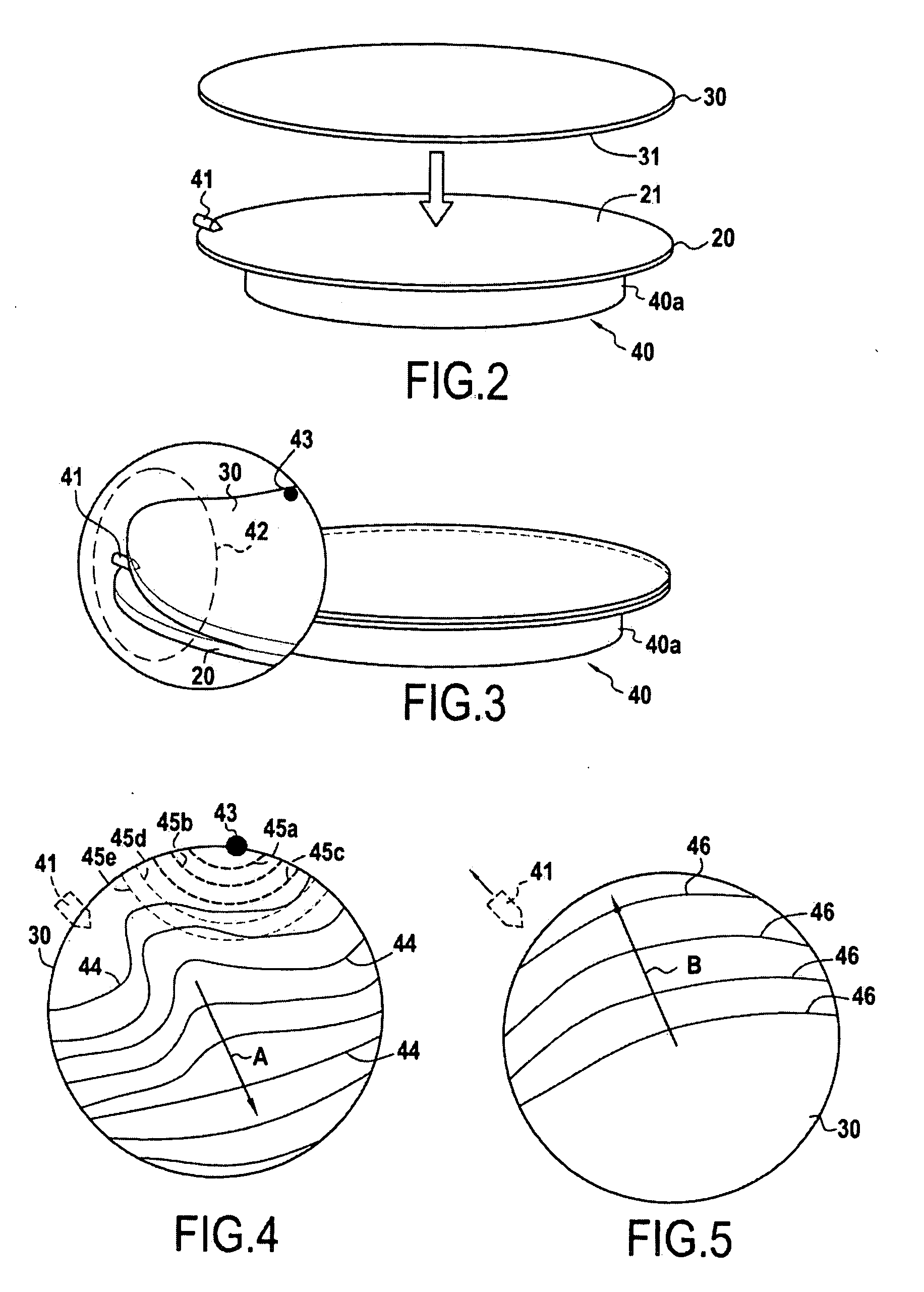
[0030]This invention applies generally to the production of composite structures including at least a bonding by molecular adhesion of a first substrate or wafer onto a second plate substrate or wafer. Bonding by molecular adhesion is a well-known technique. The principle of bonding by molecular adhesion is based on the direct contact of two surfaces, (i.e. without the use of a specific material (glue, wax, solder, etc.)). Bonding operations require that the surfaces are sufficiently smooth, free of particles and contamination, and that the surfaces are sufficiently close to one another to allow contact to be initiated, typically at a distance of less than a few nanometers. When brought into such proximity, the forces of attraction between...


PUM

PropertyMeasurementUnit
Pressureaaaaaaaaaa
Adhesion strengthaaaaaaaaaa
Areaaaaaaaaaaa

Abstract

The invention relates to a process of bonding by molecular adhesion of two layers, such as wafers of semiconductor material, wherein propagation of a first bonding wave is initiated from a pressure point applied to at least one of the two layers, and wherein the first bonding wave step is followed by propagating a second bonding wave over an area, for example, in the vicinity of the pressure point. Propagation of the second bonding wave may be obtained through the interposing of a separation element between the two wafers and the withdrawal of the element, for example, after the beginning of the first bonding wave propagation.

Description

CROSS-REFERENCE TO RELATED APPLICATION[0001]This application claims the benefit of priority from French Patent Application Serial No. FR0852990 filed May 6, 2008. The disclosure of this application is incorporated by reference herein in its entirety.BACKGROUND OF THE INVENTION[0002]1. Field of the Invention[0003]The present invention relates to the field of the production of wafers or multilayer semiconductor substrates (also called “multilayer semiconductor wafers”) effected by the transfer of at least one layer formed from an initial substrate onto a final substrate where the layer transferred corresponds to a portion of the initial substrate. The layer transferred may also include all or part of a component or a number of microcomponents.[0004]2. Description of Related Art[0005]More specifically, this invention relates to the problem of heterogeneous distortions that appear when transferring a layer from a substrate called the “donor substrate” onto a final substrate called the “...

Claims


Application Information

Patent Timeline
IPC IPC(8): H01L21/50H01L31/00
CPCC03C27/00H01L21/187H01L21/76256H01L25/0657H01L27/1464H01L27/146H01L2924/0002H01L25/50H01L2924/00
Inventor BROEKAART, MARCELASPAR, BERNARDBARGE, THIERRYBLANCHARD, CHRYSTELLE L.
Owner S O I TEC SILICON ON INSULATOR THECHNOLOGIES
Why Eureka
Try Eureka