Semiconductor device having principal surface of polar plane and side surface at specific angle to nonpolar plane and manufacturing method of the same

a technology of polar plane and side surface, which is applied in the direction of semiconductor devices, basic electric elements, electrical devices, etc., can solve the problems of reducing the yield of semiconductor devices

Inactive Publication Date: 2009-11-19
ROHM CO LTD
View PDF0 Cites 10 Cited by
  • Summary
  • Abstract
  • Description
  • Claims
  • Application Information

AI Technical Summary

Problems solved by technology

However, when the substrate is cleaved along planes other than the easiest cleavage planes in order to obtain chips having rectangular principal surfaces, cracks occur around the cutting places i

Method used


Image

  • Semiconductor device having principal surface of polar plane and side surface at specific angle to nonpolar plane and manufacturing method of the same
  • Semiconductor device having principal surface of polar plane and side surface at specific angle to nonpolar plane and manufacturing method of the same
  • Semiconductor device having principal surface of polar plane and side surface at specific angle to nonpolar plane and manufacturing method of the same

Examples


Embodiment Construction

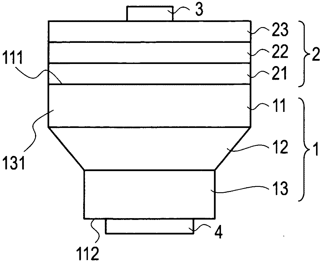
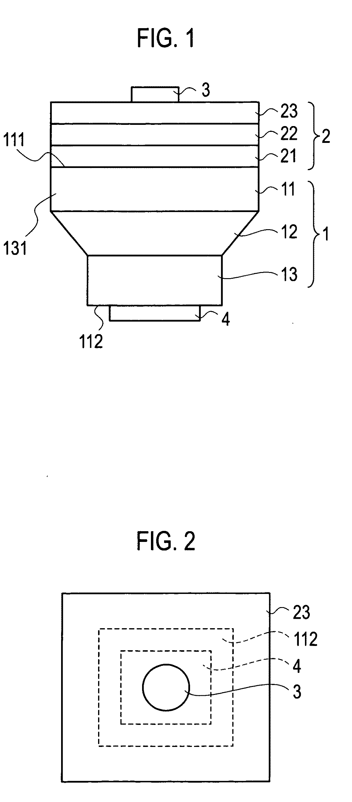
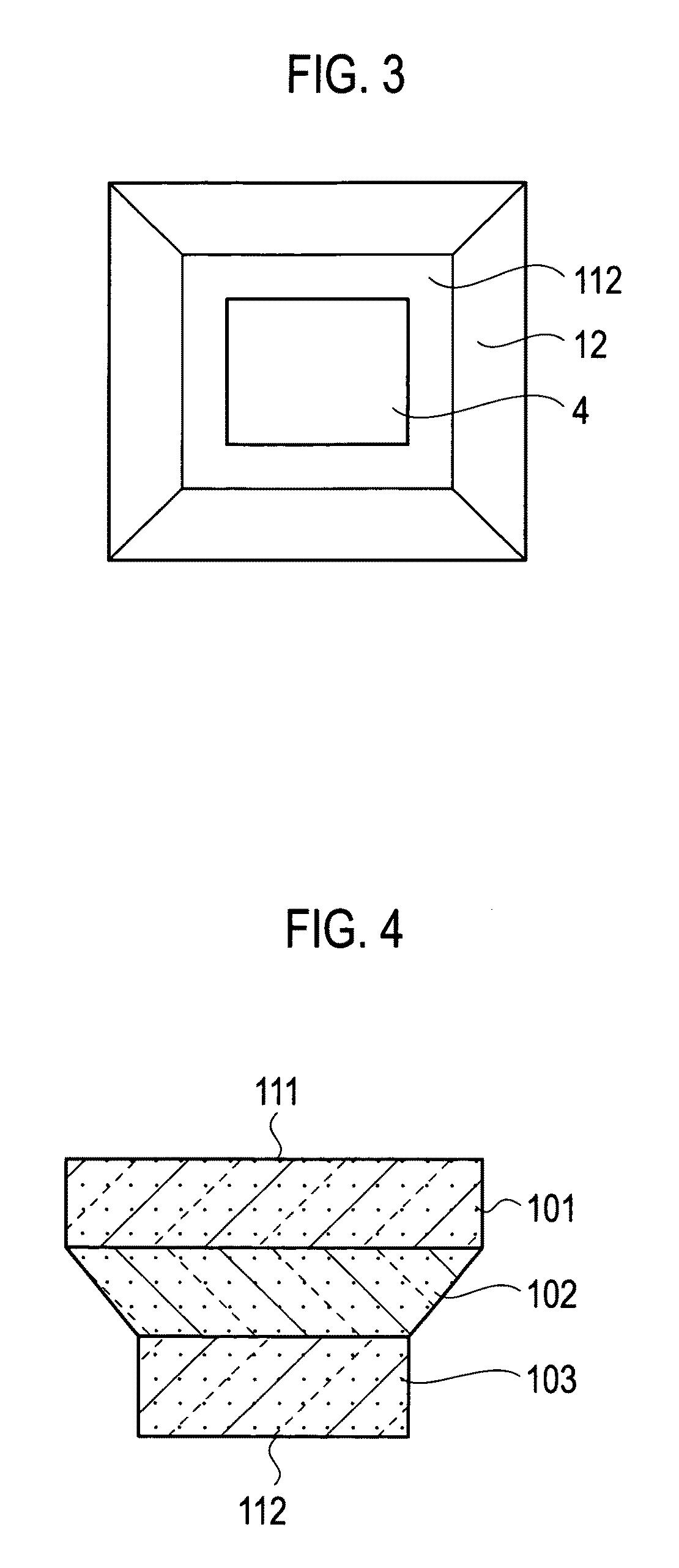
[0030]Various embodiments of the present invention will be described with reference to the accompanying drawings. It is to be noted that the same or similar reference numerals are applied to the same or similar parts and elements throughout the drawings, and the description of the same or similar parts and elements will be omitted or simplified.

[0031]Generally and as it is conventional in the representation of semiconductor devices, it will be appreciated that the various drawings are not drawn to scale from one figure to another nor inside a given figure.

[0032]In the following descriptions, numerous specific details are set forth such as specific signal values, etc., to provide a thorough understanding of the present invention. However, it will be obvious to those skilled in the art that the present invention may be practiced without such specific details.

[0033]As shown in FIG. 1, a semiconductor device according to an embodiment of the present invention includes: a substrate 1; an...


PUM


Abstract

A semiconductor device includes a substrate which is composed of a zinc oxide semiconductor having a hexagonal crystal structure and includes a first principal surface which is a polar plane; and four side surfaces which are adjacent to the first principal surface, the side surfaces being orthogonal to the principal surface and are at angles of 40 to 50 degrees to a base nonpolar plane orthogonal to the first principal surface; and a semiconductor layer provided on the first principal surface.

Description

CROSS REFERENCE TO RELATED APPLICATIONS AND INCORPORATION BY REFERENCE[0001]This application is based upon and claims the benefit of priority from prior Japanese Patent Application P2007-206939 filed on August 8, 2007; the entire contents of which are incorporated by reference herein.BACKGROUND OF THE INVENTION[0002]1. Field of the Invention[0003]The present invention relates to a semiconductor device including a zinc oxide substrate having a polar plane as a principal surface and a method of manufacturing of the same.[0004]2. Description of the Related Art[0005]A zinc oxide (ZnO) crystal is a direct transition semiconductor having a band gap of about 3.4 eV. In the ZnO crystal, a binding energy of an exciton, which is a bound state of a hole and an electron in a solid, is as large as 60 meV. The exciton in the ZnO crystal therefore exists stably even at room temperature. Accordingly, the ZnO crystal is cheep, has low environmental load, and is expected to be applied to light emitti...

Claims


Application Information

Patent Timeline
IPC IPC(8): H01L29/22H01L21/304H01L21/18H01L33/28H01L33/36
CPCH01L21/02403H01L21/02433H01L21/02554H01L21/02565H01L33/28H01L29/045H01L29/22H01L33/0095H01L33/16H01L21/78
Inventor FUJII, TETSUO
Owner ROHM CO LTD
Why Eureka
Try Eureka