Photodiode Assembly With Improved Electrostatic Discharge Damage Threshold

a photodiode and electrostatic discharge technology, applied in the field of photodiodes, can solve the problems of photodiodes and other sensitive electronic devices, easy damage to commercially available photodiodes, and fast electric transients of a few thousand volts

Inactive Publication Date: 2009-11-19
JDS UNIPHASE CORP
View PDF14 Cites 19 Cited by
  • Summary
  • Abstract
  • Description
  • Claims
  • Application Information

AI Technical Summary

Problems solved by technology

However, presently many commercially available photodiodes are susceptible to damage due to a discharge of static electricity from a neighboring object such as a human body.
The electrostatic discharge, or ESD, can result in a fast electric transient of a few thousand Volts and is one of the common causes of failure of photodiodes and other sensitive electronic devices.
These measures are expensive to implement and are not completely effective, with residual ESD damage being sometimes difficult to detect.
Furthermore, an ESD can damage the photodiodes at a customer site, if similar precautionary measures are not implemented.

Method used


Image

  • Photodiode Assembly With Improved Electrostatic Discharge Damage Threshold
  • Photodiode Assembly With Improved Electrostatic Discharge Damage Threshold
  • Photodiode Assembly With Improved Electrostatic Discharge Damage Threshold

Examples


Embodiment Construction

[0024]While the present teachings are described in conjunction with various embodiments and examples, it is not intended that the present teachings be limited to such embodiments. On the contrary, the present teachings encompass various alternatives, modifications and equivalents, as will be appreciated by those of skill in the art.

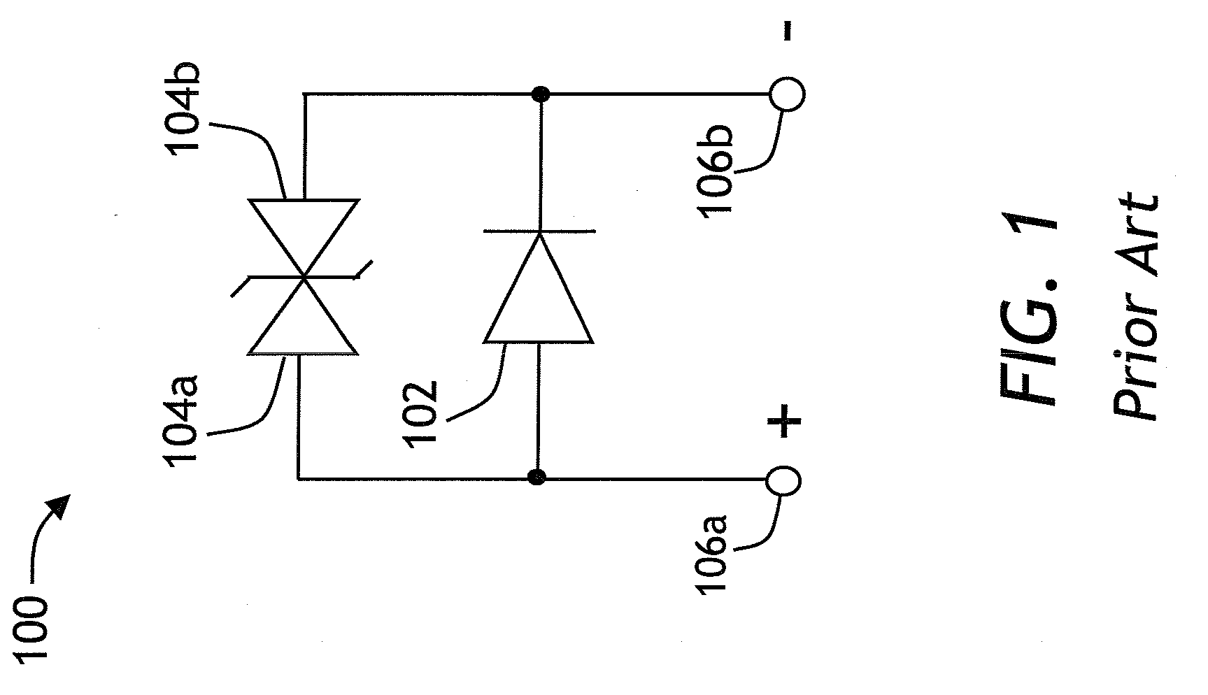
[0025]FIG. 1 shows a prior art protection circuit 100 for a light emitting diode, or LED 102, comprising a pair of Zener diodes 104a and 104b connected in parallel to LED 102. In operation, a voltage is applied to electrodes 106a and 106b so as to make LED 102 emit light. Since Zener diodes 104a and 104b are connected cathode-to-cathode, they exhibit high electric resistance and, therefore, in operation, almost all of the electric current flows through LED 102. When an ESD pulse of either polarity arrives, the Zener diodes 104a and 104b conduct, short-circuiting the path of electric current and protecting LED 102.

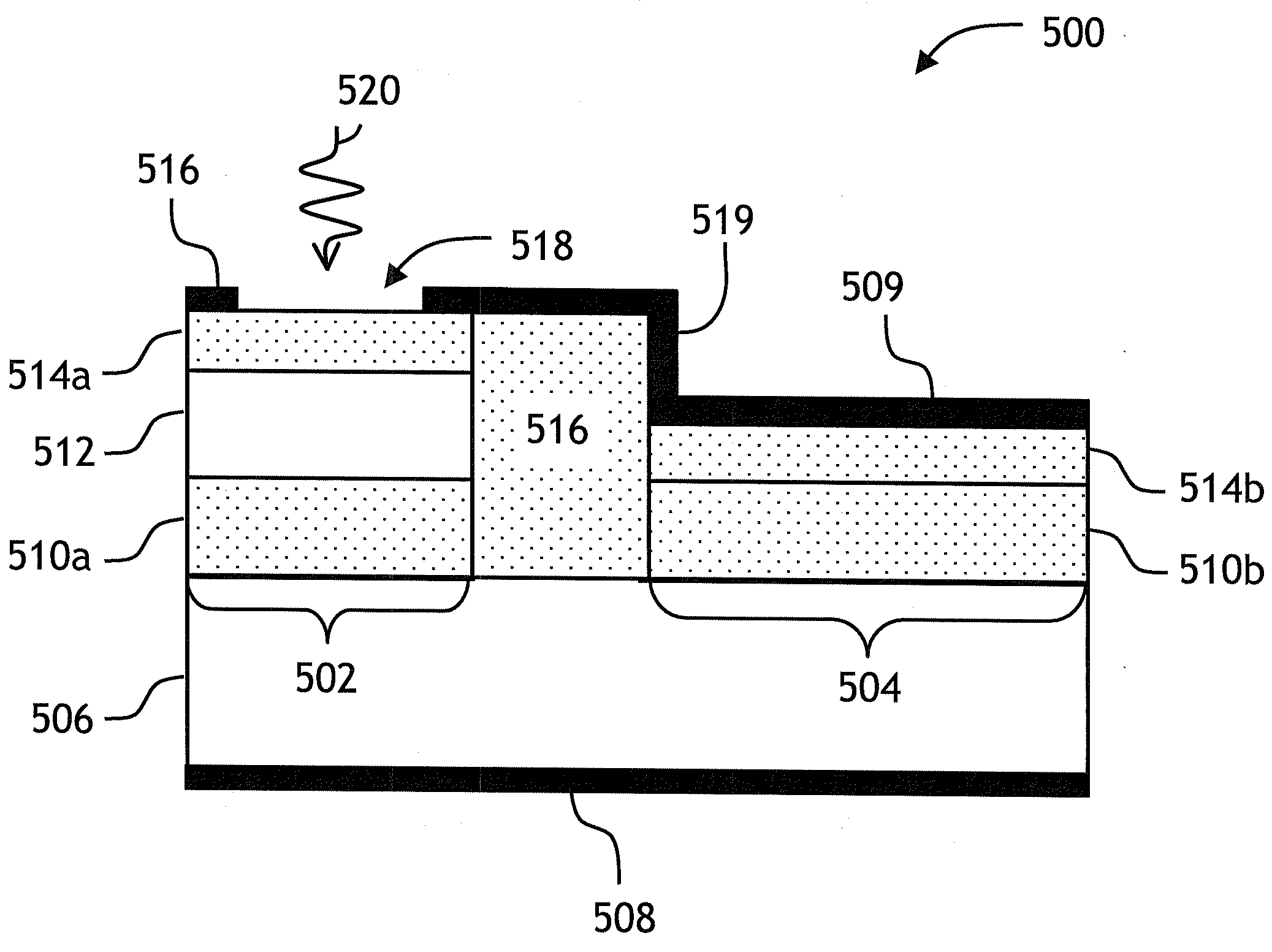
[0026]Turning now to FIG. 2, a top view of...


PUM


Abstract

A photodiode with an improved electrostatic damage threshold is disclosed. A Zener or an avalanche diode is connected in parallel to a photodiode. Both diodes are integrated into the same photodiode housing. The diodes can be mounted on a common header or onto each other. An avalanche photodiode and an avalanche diode can be fabricated on a common semiconductor substrate. A regular p-n diode connected in series, cathode-to-cathode or anode-to-anode, to a Zener diode, forms a protection circuit which, when connected in parallel to a photodiode, provides a smaller electrical capacity increase as compared to a simpler circuit consisting just of a Zener or an avalanche diode.

Description

TECHNICAL FIELD[0001]The present invention is related to photodiodes, and specifically to photodiodes having high electrostatic damage threshold.BACKGROUND OF THE INVENTION[0002]Photodiodes are semiconductor photodetectors capable of converting light into electric current or voltage. The most commonly used photodetectors are positive-negative (p-n) photodiodes, positive-intrinsic-negative (p-i-n) photodiodes, and avalanche photodiodes.[0003]A photon absorbed at a p-n junction of a p-n photodiode, or at an intrinsic region, or i-region, of a p-i-n photodiode, generates a pair of current carriers, a hole in the valence band and the electron in the conduction band, which drift towards respective p- and n-doped areas. When reverse biased with an external voltage source, a photodiode converts light into a current. When left unbiased, a photodiode generates a small voltage, of the order of one Volt, in response to light. An avalanche photodiode is, in its simplest form, a p-i-n diode with...

Claims


Application Information

Patent Timeline
Patent Type & Authority Applications(United States)
IPC IPC(8): H01L29/866
CPCH01L27/0248H01L2224/48091H01L2224/48137H01L2224/48472H01L2224/73265H01L2924/00014
Inventor TAN, I-HSINGSHANG, SHUPINGBOUEVITCH, OLEG
Owner JDS UNIPHASE CORP
Why Eureka
Try Eureka