Dll circuit adapted to semiconductor device
a dll circuit and semiconductor technology, applied in the direction of pulse manipulation, pulse automatic control, pulse technique, etc., can solve the problems of increasing the number of cycles adapted to delay-locked control, difficult to precisely perform phase detection and duty detection, and the dll clock signal to disappear temporarily, so as to reduce the number of cycles and stabilize the operation of the dll circuit
- Summary
- Abstract
- Description
- Claims
- Application Information
AI Technical Summary
Benefits of technology
Problems solved by technology
Method used
Image

Examples
first embodiment
1. First Embodiment
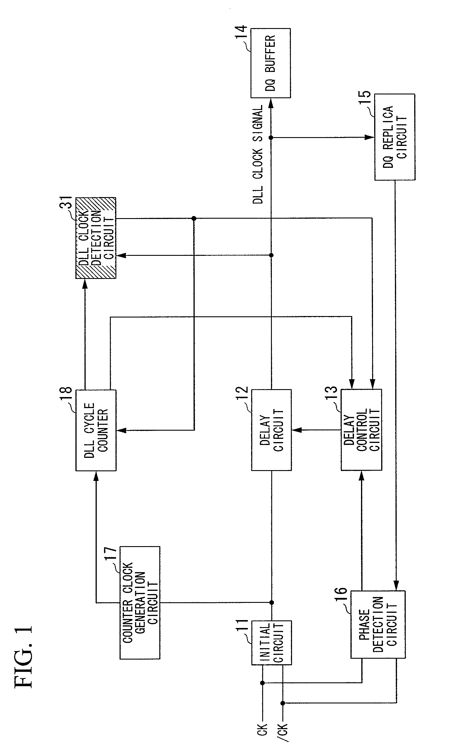
[0053]FIG. 1 shows a DLL circuit according to a first embodiment of the present invention, which is designed to perform the phase control only, wherein parts identical to those shown in FIG. 9 are designated by the same reference numerals. The DLL circuit of FIG. 1 includes a DQ buffer 14 whose output signal is synchronized with the clock signal CK and the inverse clock signal / CK by correcting a delay time.
[0054]In FIG. 1, the initial circuit 11 receives a differential input signal corresponding to the clock signals CK and / CK, thus producing a clock signal for the DLL circuit. The clock signal output from the initial circuit 11 is supplied to the delay circuit 12 and the counter clock generation circuit 17.
[0055]The counter clock generation circuit 17 divides the frequency of the clock signal so as to generate and output a counter clock signal (see FIG. 5A) to the DLL cycle counter 18.
[0056]The delay circuit 12 includes a plurality of delay elements, one of whic...
second embodiment
2. Second Embodiment
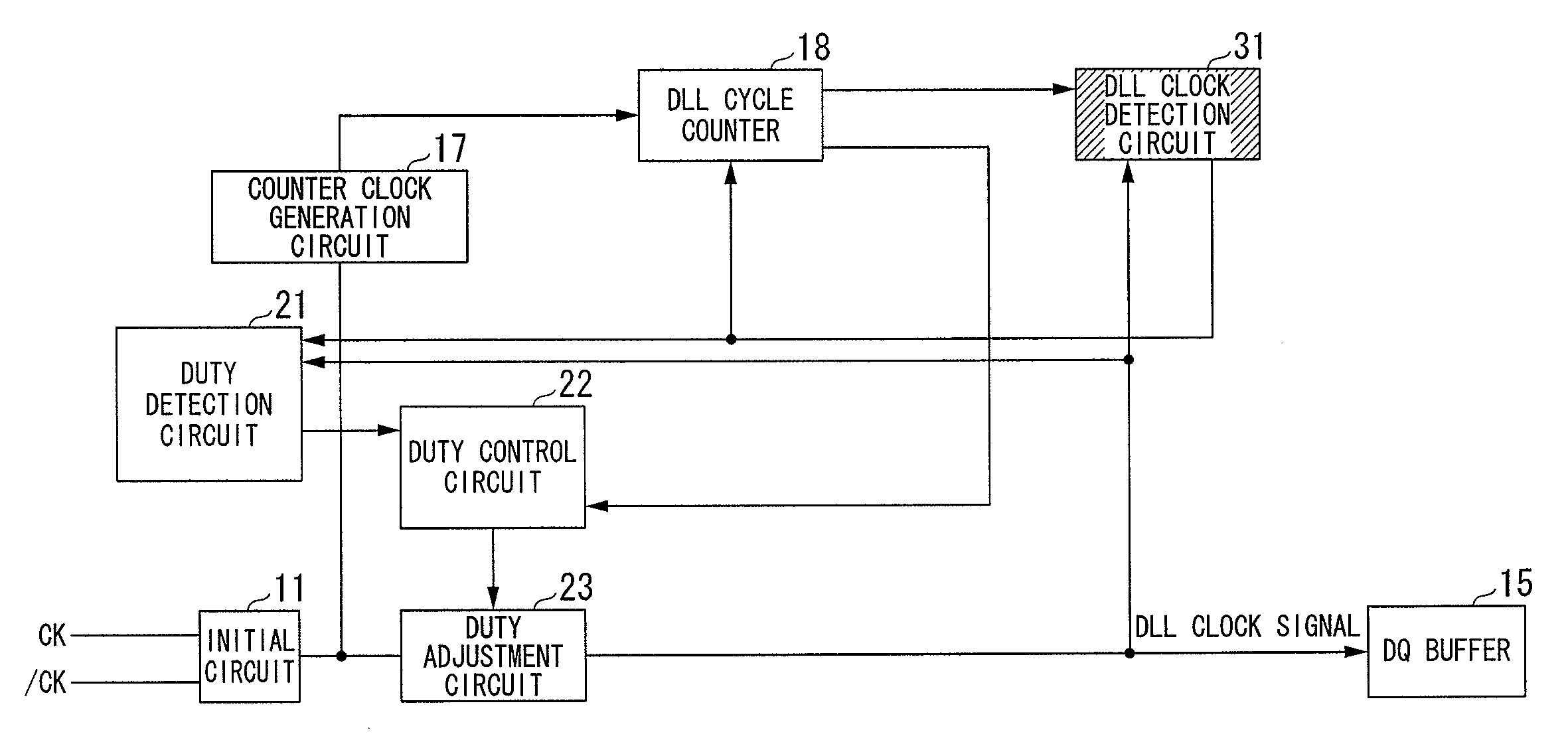
[0066]FIG. 2 shows a DLL circuit according to a second embodiment of the present invention, which is designed to perform the duty control only, wherein parts identical to those shown in FIGS. 1 and 9 are designated by the same reference numerals.
[0067]In FIG. 2, the initial circuit 11 converts a differential input signal (corresponding to the clock signals CK and / CK) into a clock signal for use in the DLL circuit. The clock signal output from the initial circuit 11 is supplied to the counter clock generation circuit 17 and the duty adjustment circuit 23.
[0068]The counter clock generation circuit 17 divides the frequency of the clock signal so as to generate and output the counter clock signal (see FIG. 5A) to the DLL cycle counter 18.
[0069]The duty detection circuit 21 performs detection as to whether the duty of the DLL clock signal is above or below 50%. Based on the duty detection result output from the duty detection circuit 21, the duty control circuit 22 p...
third embodiment
3. Third Embodiment
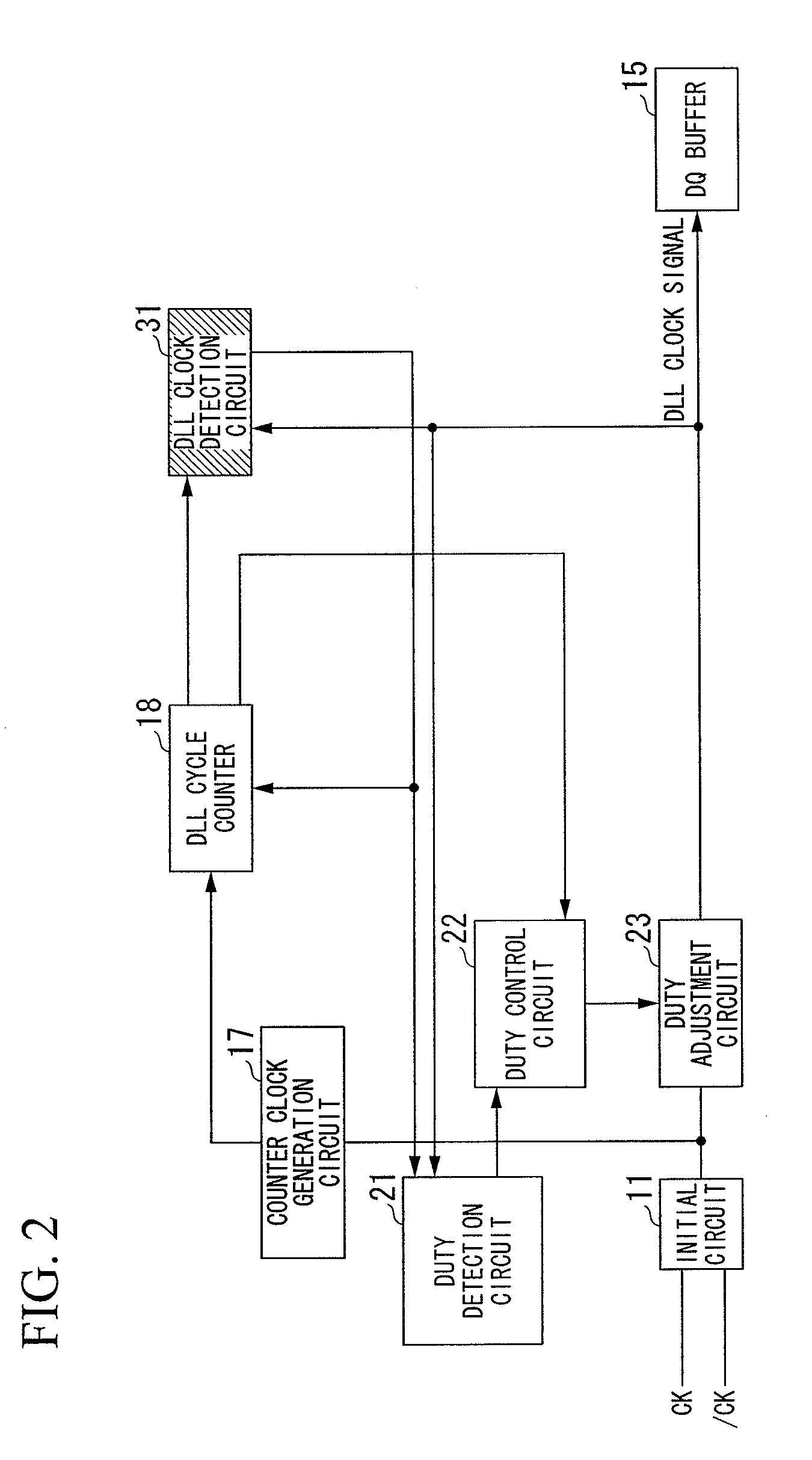
[0078]FIG. 3 shows a DLL circuit according to a third embodiment of the present invention, wherein parts identical to those shown in FIGS. 1, 2, and 9 are designated by the same reference numerals. The DLL circuit of FIG. 3 is designed to perform both the phase control and the duty control, wherein it is a combination of the DLL circuit of FIG. 1 achieving the phase control and the DLL circuit of FIG. 2 achieving the duty control.
[0079]The duty adjustment circuit 23 adjusts the duty of the clock signal of the initial circuit 11 such that the duty of an internal clock signal used in the DQ buffer 14 becomes equal to or close to 50%. The delay circuit 12 corrects the delay time imparted to the duty-adjusted clock signal output from the duty adjustment circuit 23 such that the DQ output signal of the DQ buffer 14 is synchronized with the clock signals CK and / CK, thus outputting the DLL clock signal to the DQ buffer 14.
[0080]The DLL clock signal is supplied to the DQ...
PUM
 Abstract
Description
Claims
Application Information
 - R&D
- Intellectual Property
- Life Sciences
- Materials
- Tech Scout
- Unparalleled Data Quality
- Higher Quality Content
- 60% Fewer Hallucinations
Browse by: Latest US Patents, China's latest patents, Technical Efficacy Thesaurus, Application Domain, Technology Topic, Popular Technical Reports.
© 2025 PatSnap. All rights reserved.Legal|Privacy policy|Modern Slavery Act Transparency Statement|Sitemap|About US| Contact US: help@patsnap.com