Analysis of stress impact on transistor performance

a technology of stress and transistor performance, applied in the direction of error detection/correction, instruments, cad circuit design, etc., can solve the problems of increasing computation time required to obtain accurate, increasing increasing the amount of piezoelectric effect on transistor performance. achieve the effect of reducing the amount of oxide, reducing the actual stress in the channel, and reducing computation costs

Active Publication Date: 2009-11-19
SYNOPSYS INC
View PDF23 Cites 17 Cited by
  • Summary
  • Abstract
  • Description
  • Claims
  • Application Information

AI Technical Summary

Benefits of technology

[0010]Fourth, the LOD model fails to take into account the presence of other structures in the neighborhood of a region under study, apart from the nearest STI interface. Other structures beyond this interface might reduce the amount of oxide presumed to be exerting a force, and therefore might reduce the actual stress in the channel.
[0011]Accordingly, it would be extrem...

Problems solved by technology

As process technologies have continued to shrink, however, the piezoelectric effect on transistor performance is no longer negligible.
The computation time required to obtain accurate results, however, limited the utility of this kind of analysis to only small regions of a chip layout that include only several transistors.
For example, it has not been practical to perform a TCAD analysis to obtain reasonably accurate circuit level parameters for layout regions larger than about a dozen transistors, or about 2-3 diffusion regions.
Even then, huge amounts of CPU time, up to several hours per transistor, were required to obtain reasonably accurate results.
The required computation time makes this approach prohibitively exp...

Method used


Image

  • Analysis of stress impact on transistor performance
  • Analysis of stress impact on transistor performance
  • Analysis of stress impact on transistor performance

Examples


Embodiment Construction

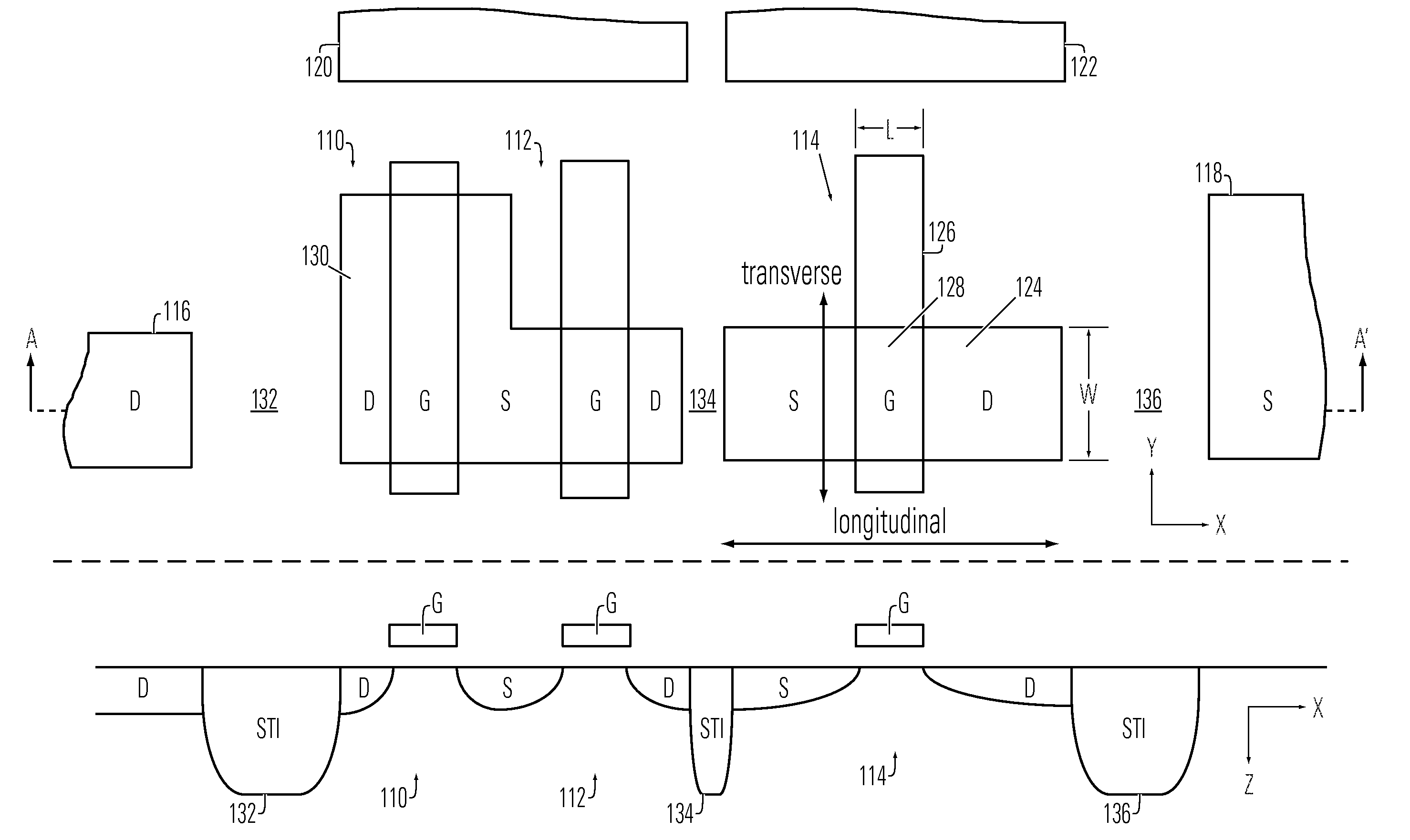
[0017]In order to best describe an embodiment of the invention, reference will be made to an illustrative layout portion as shown in FIG. 1. In FIG. 1, the top portion of the diagram illustrates a plan view of the layout region, and the bottom portion of the diagram illustrates a cross-section taken at sight-line A-A′ as shown in the top portion. The layout region of FIG. 1 includes three transistors 110, 112 and 114, plus some other structures 116, 118, 120 and 122. Referring to transistor 114 as an example, it comprises a diffusion region 124 which is crossed by a gate conductor 126. The portion of the diffusion region 124 to the left of the gate 126 is the source diffusion region of the transistor, and the portion to the right of the gate 126 is the drain diffusion region. The portion of the diffusion region 124 overlapping with below the gate 126 is the channel 128 of the transistor. As used herein, the term “region” represents a two-dimensional area in a plan view of the layout...


PUM


Abstract

Roughly described, a method for approximating stress-induced mobility enhancement in a channel region in an integrated circuit layout, including approximating the stress at each of a plurality of sample points in the channel, converting the stress approximation at each of the sample points to a respective mobility enhancement value, and averaging the mobility enhancement values at all the sample points. The method enables integrated circuit stress analysis that takes into account stresses contributed by multiple stress generation mechanisms, stresses having vector components other than along the length of the channel, and stress contributions (including mitigations) due to the presence of other structures in the neighborhood of the channel region under study, other than the nearest STI interfaces. The method also enables stress analysis of large layout regions and even full-chip layouts, without incurring the computation costs of a full TCAD simulation.

Description

RELATED APPLICATIONS[0001]This is a division of application Ser. No. 11 / 291,294, filed 1 Dec. 2005 which is incorporated herein in its entirety.FIELD OF THE INVENTION[0002]The invention relates to the modeling of integrated circuit devices, and more particularly to the modeling of stress impact on transistor performance.BACKGROUND AND SUMMARY OF THE INVENTION[0003]It has long been known that semiconductor materials such as silicon and germanium exhibit the piezoelectric effect (mechanical stress-induced changes in electrical resistance). See for example C. S. Smith, “Piezoresistance effect in germanium and silicon”, Phys. Rev., vol. 94, pp. 42-49 (1954), incorporated by reference herein. The piezoelectric effect has formed the basis for certain kinds of pressure sensors and strain gauges, but only recently has it received attention in the manufacture of integrated circuits. In integrated circuit fabrication, one of the major sources of mechanical stress is the differential expansion...

Claims


Application Information

Patent Timeline
IPC IPC(8): G06F17/50
CPCG06F17/5081G06F17/5036G06F30/367G06F30/33G06F30/398
Inventor MOROZ, VICTORPRAMANIK, DIPANKAR
Owner SYNOPSYS INC
Why Eureka
Try Eureka