Mold shave apparatus and injection molded soldering process

a technology of injection molding and shave apparatus, which is applied in the direction of inking apparatus, soldering apparatus, manufacturing tools, etc., can solve the problems of insufficient or empty mold cavities, adversely affecting the integrity of any electronic device, and inability to remove solder or alloy quantities at room temperature, so as to facilitate the shaving of excess solder volumes, adversely affecting the solder volume, and the effect of rapid operation

Inactive Publication Date: 2009-12-03
IBM CORP
View PDF6 Cites 6 Cited by
  • Summary
  • Abstract
  • Description
  • Claims
  • Application Information

AI Technical Summary

Benefits of technology

[0006]In order to be able to attain the foregoing, an apparatus and process pursuant to the invention is provided which facilitates removal of solder bridges, streakings and raised solder portions, without adversely affecting or removing the quantities of solder which have already solidified in the mold cavities and which are required for producing the (C4) connections. Various types of solder may also possess a weaker degree of adherence to the wall surfaces in the mold cavities, and the light pressure, which is normally needed to remove the solder bridging, streaking and contaminants from the surface of the mold may, at times, be enough so as to result in the formation of either empty or inadequately filled mold cavities, thereby adversely affecting the integrity of any electronic devices that incorporate the particular wafer or semiconductor structures formed therefrom.
[0011]In order to attain the foregoing, pursuant to the present invention, there is provided a unique apparatus which will facilitate the shaving of excess solder volumes from the surface of the mold without in any manner adversely affecting the solder volume which has already been filled into the mold cavities, by heating a shaving blade and mold plate.
[0012]In essence, the known injection molded solder transfer process cannot allow for the acceptance of large variations in solder bump volumes, and, consequently, by utilizing the inventive shaving apparatus and method, the excess volume of solder, which could adversely affect the solder bumps and also form any bridging or solder excess is removed without damage being sustained by the solder volumes contained in the respective cavities. This shaving action can also be implemented prior to inspection on all molds, even in the absence of any adverse bridging or defects, inasmuch as the inventive method and apparatus is inexpensive and rapid in operation, thereby eliminating costly inspection errors and reducing any necessary rework.

Problems solved by technology

Generally, in the current technology, which is concerned with the process of injection molding, it is readily acknowledged that some amounts of solder or alloys cannot be removed at room temperature without concurrently causing the removal of some solder which is filled in the mold cavities.
Various types of solder may also possess a weaker degree of adherence to the wall surfaces in the mold cavities, and the light pressure, which is normally needed to remove the solder bridging, streaking and contaminants from the surface of the mold may, at times, be enough so as to result in the formation of either empty or inadequately filled mold cavities, thereby adversely affecting the integrity of any electronic devices that incorporate the particular wafer or semiconductor structures formed therefrom.
Other problems encountered in the technology are that some solders are naturally harder, for example, such as solders containing high amounts of tin (Sn) for providing a lead-free structure, whereby these high tin solders cannot be easily removed by means of a shaving blade or removal instrument at room temperature, and wherein the cutting edge force acting on the solder streaks or bridges may exceed the adherence of the solder to some of the cavities provided in the mold.

Method used


Image

  • Mold shave apparatus and injection molded soldering process
  • Mold shave apparatus and injection molded soldering process

Examples


Embodiment Construction

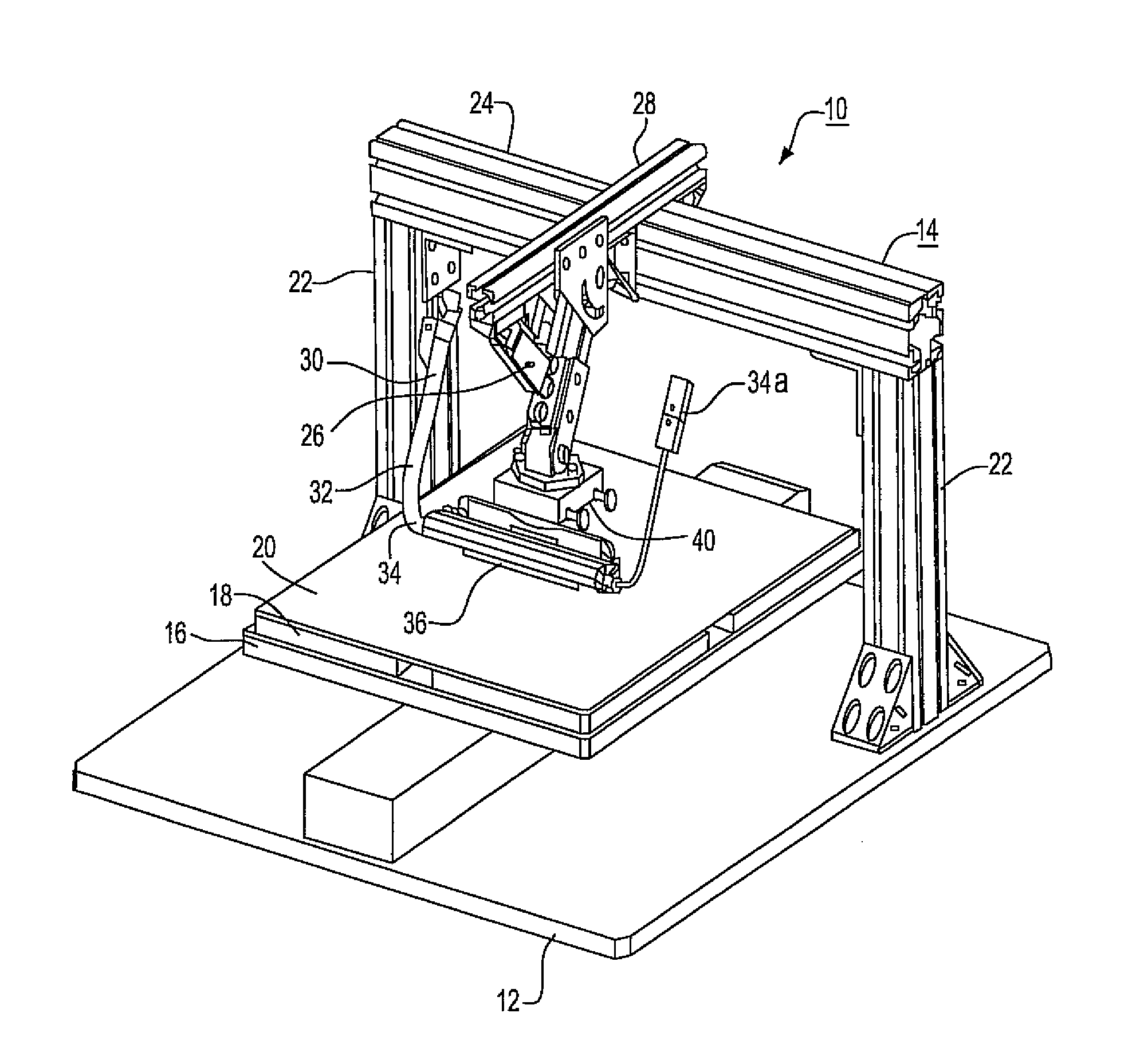
[0014]Referring to the shaving apparatus 10, there is disclosed a plate-like bottom support member 12 that has an upright bridge frame structure 14 beneath which there is located a movable table 16 adapted to be displaced in both x and y directions along the bottom support member 12 through the operation of a suitable operating and conveying structure (not shown).

[0015]Supported on the movable table 16 is a vacuum table 18, which enables the retention thereon of a large-sized mold plate 20 with a surface having a multiplicity of cavities or small holes (not shown) formed therein; each of which is adapted to be filled with a quantity of molten solder possessed of a precise volume of (C4) bumps, which are to be transferred to suitable wafer pads (not shown). As indicated, the mold plate 20 may be constituted of a borosilicate glass plate having the cavities etched therein, which represent the wafer (C4) pad locations and with cavity quantities ranging of from 100,000 to an excess of 1...


PUM

PropertyMeasurementUnit
diameteraaaaaaaaaa
diameteraaaaaaaaaa
volumeaaaaaaaaaa

Abstract

An apparatus for the removal of excess solder or contaminant, which are encountered on the surfaces of injection mold prior to the transfer of a solder on a silicon wafer. More particularly, there is provided an apparatus for the removal of excess solder, which may be present on a mold surface, without removing any solder, which is located in cavities formed in the mold, and wherein the solder is applied through an injection molded soldering process.

Description

CROSS REFERENCE TO RELATED PATENT APPLICATION[0001]This application is a divisional of U.S. Ser. No. 11 / 619,197, filed on Jan. 3, 2007.BACKGROUND OF THE INVENTIONField of the Invention[0002]The present invention relates to an apparatus and to a method for the removal of excess solder or contaminant which are encountered on the surfaces of injection mold prior to the transfer of a solder on a silicon wafer. More particularly, the present invention is directed to the removal of excess solder, which may be present on a mold surface, without removing any solder, which is located in cavities formed in the mold, and wherein the solder is applied through an injection molded soldering process.[0003]During the application of quantities of molten solder over the surface of a mold plate possessing cavities which are adapted to be filled with the molten solder, wherein the cavities represent wafer controlled collapse chip connecting (C4) pad locations, quite frequently the surface of the mold i...

Claims


Application Information

Patent Timeline
Patent Type & Authority Applications(United States)
IPC IPC(8): B22D11/126
CPCB23K2201/42B23K3/08B23K2101/42
Inventor BOUCHARD, ERIC E.BROUILLETTE, GUYDANOVITCH, DAVID H.GRUBER, PETER A.LANDREVILLE, JEAN-LUC
Owner IBM CORP
Why Eureka
Try Eureka