Liquid crystal blind, method of manufacturing semiconductor device using the same, and reduced projection exposure apparatus

Inactive Publication Date: 2009-12-03
SEIKO EPSON CORP
View PDF4 Cites 0 Cited by
  • Summary
  • Abstract
  • Description
  • Claims
  • Application Information

AI Technical Summary

Benefits of technology

[0019]Therefore, an advantage of the invention is to flexibly control the irradiation light applied on the reticle.
[0020]A liquid crystal blind according to a first aspect of the invention includes a transparent first electrode layer, a transparent second electrode layer intersecting with the first electrode layer, and a liquid crystal cell formed between the first electrode layer and the second electrode layer, wherein the liquid crystal blind has an irradiation pattern, and a voltage is applied between the first electrode layer and the second electrode layer, thereby setting an irradiation area adapted to apply irradiation light to a semiconductor substrate and determining the irradiation pattern.
[0021]Further, in the liquid crystal blind described above, the liquid crystal cell can be controlled so as to determine an irradiation time in accordance with the irradiation area.
[0022]A method of manufacturing a semiconductor device according to another aspect of the invention is a method of manufacturing a semiconductor device using a liquid crys

Problems solved by technology

In the case of the reduced projection exposure apparatus, since the irradiation area of the irradiation light applied on the reticle is set by driving the four segments, namely the top, bottom, left, and right segments of the blind in the predetermined directions, there is caused inconvenience that the shape of the opening section is limited to a rectangle, but not allowed to be set arbitrarily.
Further, since the shape of the opening section of the blind is fixed during the period in which the shutter is opened to apply the irradiation light, there is also caused inconvenience that it is not allowed to arbitrarily set the irradiation time in accordance with the irradiation area on the reticle.
Further, since the projection and exposure are performed in the product pattern area defined within the projection area on the reticle to which the same irradiation time is applied, there also arises a problem that the dimensional accuracy of the resist pattern image of the product chips existing in the product pattern area and thus projected and exposed is degraded in the

Method used


Image

  • Liquid crystal blind, method of manufacturing semiconductor device using the same, and reduced projection exposure apparatus
  • Liquid crystal blind, method of manufacturing semiconductor device using the same, and reduced projection exposure apparatus
  • Liquid crystal blind, method of manufacturing semiconductor device using the same, and reduced projection exposure apparatus

Examples


Example

First Embodiment

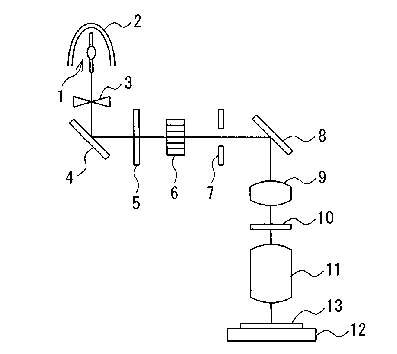
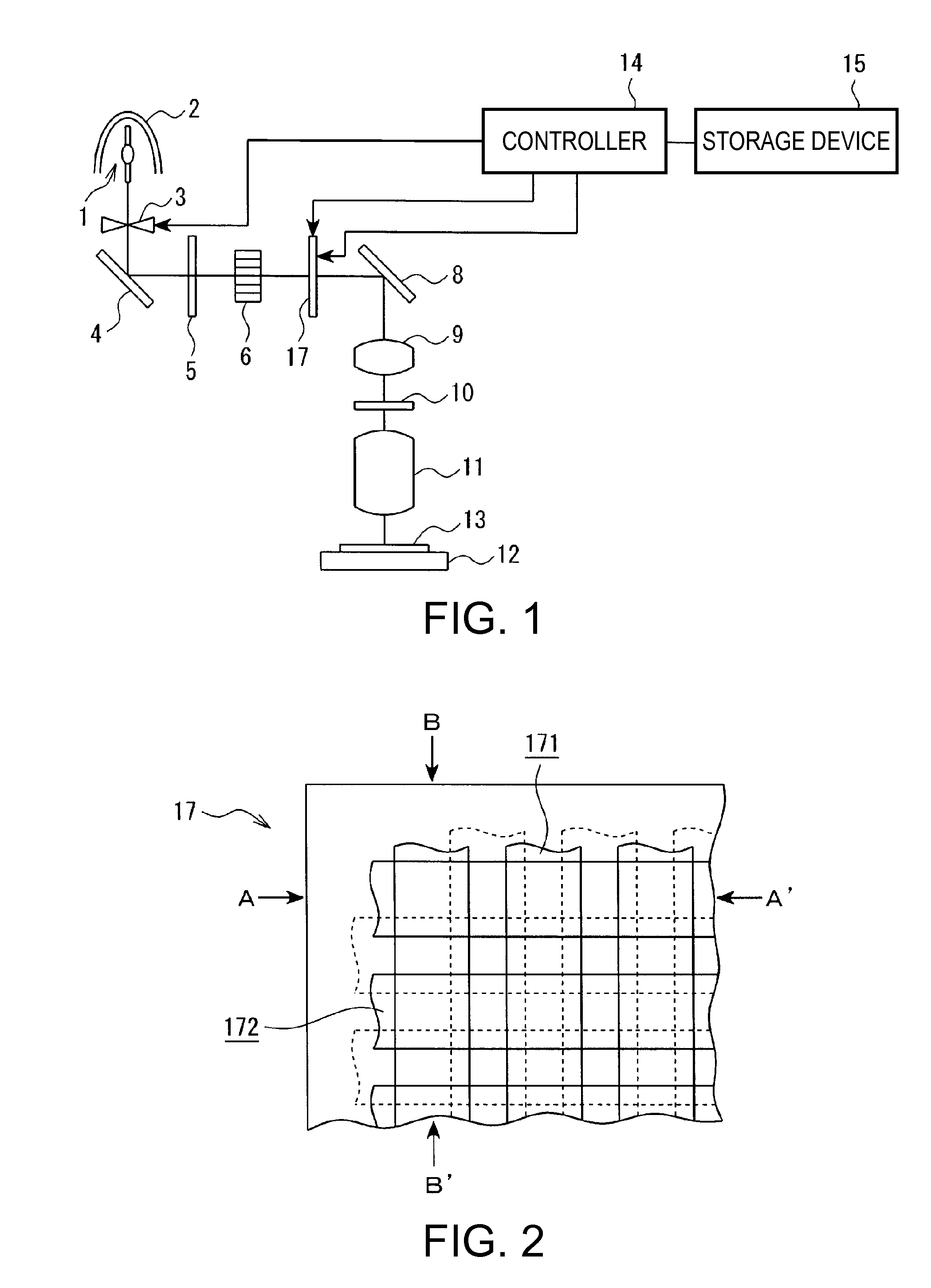
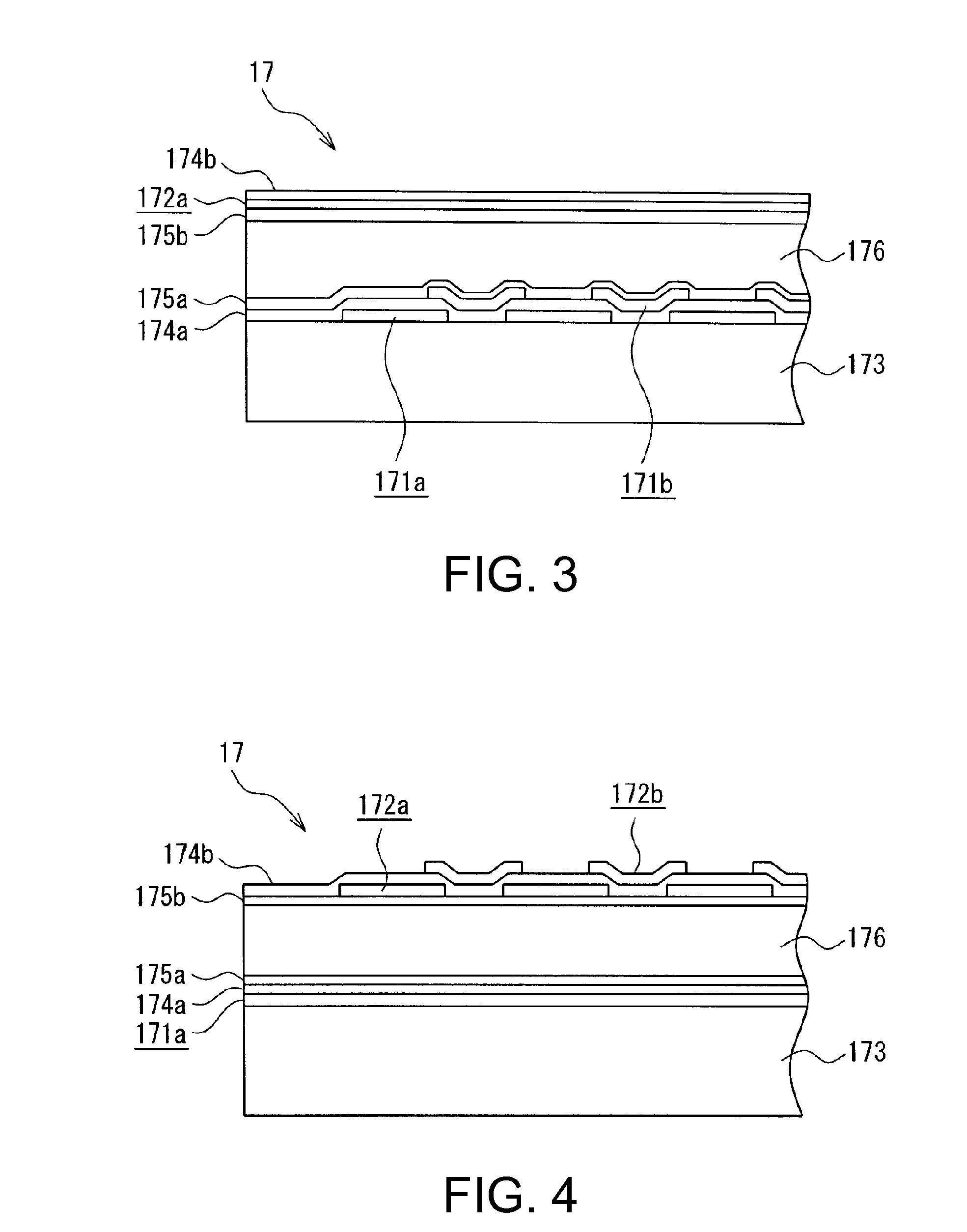
[0050]FIG. 1 is a schematic diagram showing a basic configuration of a reduced projection exposure apparatus according to the first embodiment of the invention. Further, FIG. 2 is a plan view showing a fundamental structure of a liquid crystal blind 17 as an essential part of the reduced projection exposure apparatus with a part thereof broken.

[0051]The reduced projection exposure apparatus is provided with a mercury lamp 1 as a source of luminescence, an elliptical mirror 2 for reflecting and collecting the light emitted by the mercury lamp 1 to form irradiation light, a shutter 3 for controlling the irradiation time of the irradiation light in accordance with an open / closed state, a total reflection mirror 4 for totally reflecting the irradiation light from the shutter 3 in a lengthwise direction, an interference filter 5 for transmitting the irradiation light totally reflected by the total reflection mirror 4 to select only necessary wavelengths, a fly-eye lens 6 ...

Example

Second Embodiment

[0085]In the case of the reduced projection exposure apparatus according to the first embodiment, the case in which the optical opening section of the liquid crystal blind 17 is controlled in two levels due to the action of the storage device 15 and the controller 14, thereby variably setting the shape of the irradiation area of the irradiation light is explained. In the second embodiment, the control with finer levels is performed, thereby variably setting the shape of the irradiation area.

[0086]FIGS. 8A through 8E are diagrams exemplifying the product pattern area Ep varied in accordance with the irradiation pattern on the reticle 10, on which the irradiation control by the liquid crystal blind 17 in the reduced projection exposure apparatus according to the second embodiment of the invention is conducted, wherein FIG. 8A is related to the entire area irradiation pattern, FIG. 8B is related to a first partial area irradiation pattern, FIG. 8C is related to a secon...


PUM


Abstract

A liquid crystal blind includes a transparent first electrode layer, a transparent second electrode layer intersecting with the first electrode layer, and a liquid crystal cell formed between the first electrode layer and the second electrode layer, wherein the liquid crystal blind has an irradiation pattern, and a voltage is applied between the first electrode layer and the second electrode layer, thereby setting an irradiation area adapted to apply irradiation light to a semiconductor substrate and determining the irradiation pattern.

Description

BACKGROUND[0001]1. Technical Field[0002]Several aspects of the present invention relate to a liquid crystal blind used when performing reduced projection exposure on an exposed semiconductor substrate surface, a method of manufacturing a semiconductor device to which the liquid crystal blind is applied, and a reduced projection exposure apparatus.[0003]2. Related Art[0004]As the reduced projection exposure apparatus of this kind in the related art, the apparatus (the apparatus with a configuration not the invention known to the public by literature, but conceived to generally well known to the public) with a configuration shown in FIG. 10 can be cited.[0005]In the case of this reduced projection exposure apparatus, light emitted from a mercury lamp 1 as a source of luminescence is reflected or collected by an elliptical mirror 2 to be formed as irradiation light, and the irradiation light with irradiation time controlled in accordance with an open / closed state of a shutter 3 is tota...

Claims


Application Information

Patent Timeline
IPC IPC(8): G02F1/1335
CPCG03F7/70066G02F1/134309
Inventor USHIYAMA, FUMIAKI
Owner SEIKO EPSON CORP
Why Eureka
Try Eureka