

Techniques for Three-Dimensional Circuit Integration
a three-dimensional circuit and integrated circuit technology, applied in the field of integrated circuits, can solve the problems of damage to the exposed insulator (oxide), negative affecting the quality of the subsequent oxide-to-oxide bond with the other device layer, and drawbacks associated with this type of conventional three-dimensional fabrication process
- Summary
- Abstract
- Description
- Claims
- Application Information
AI Technical Summary
Problems solved by technology
Method used
Image

Examples
Embodiment Construction
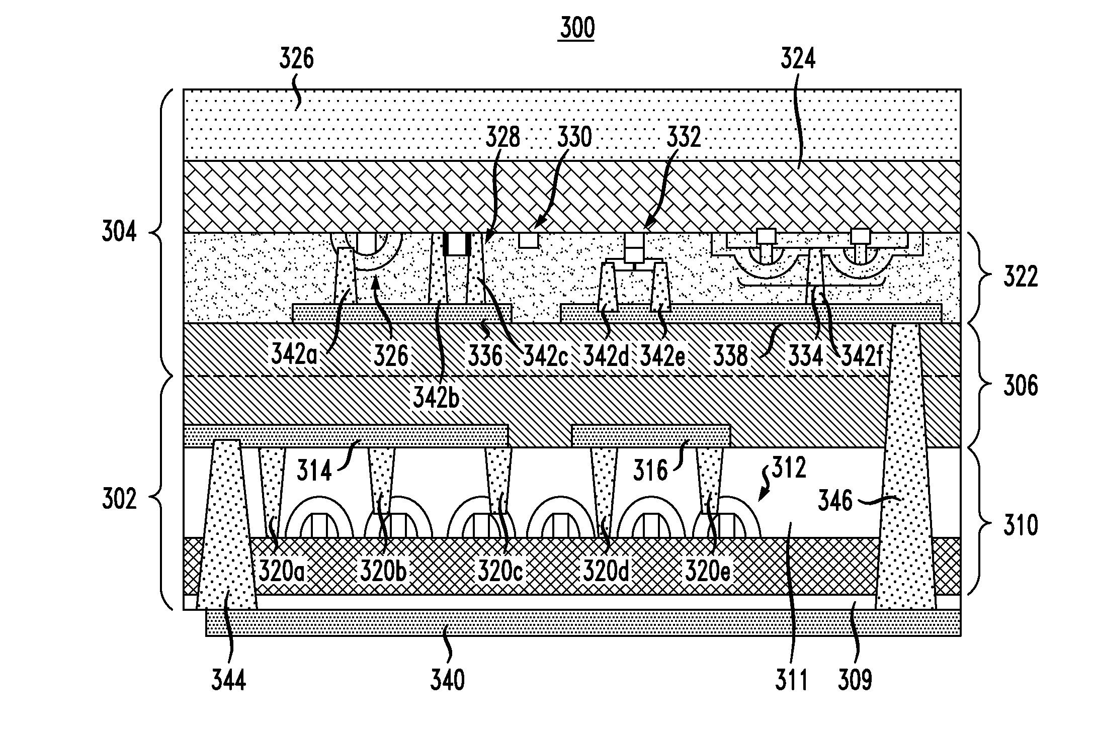
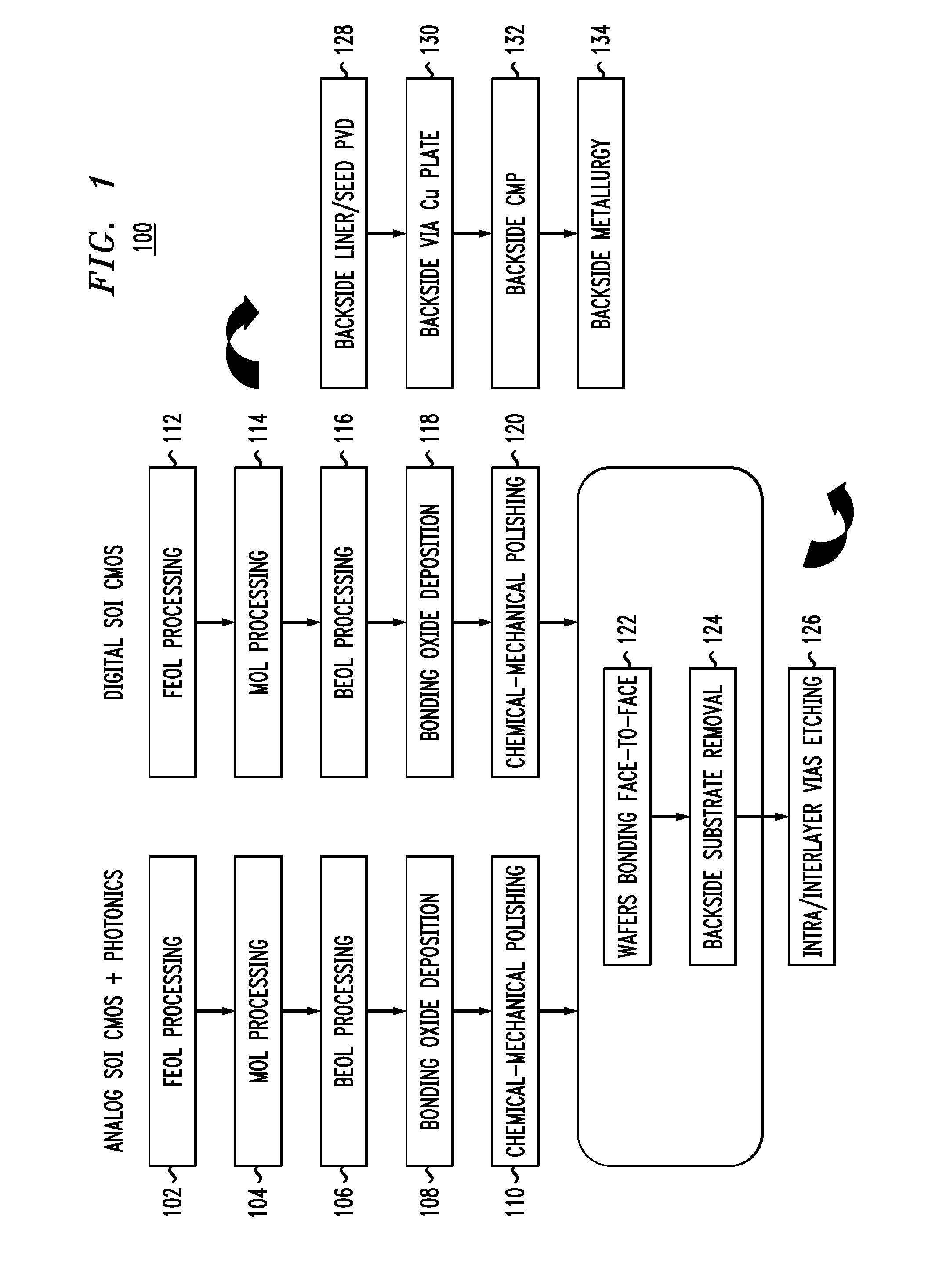
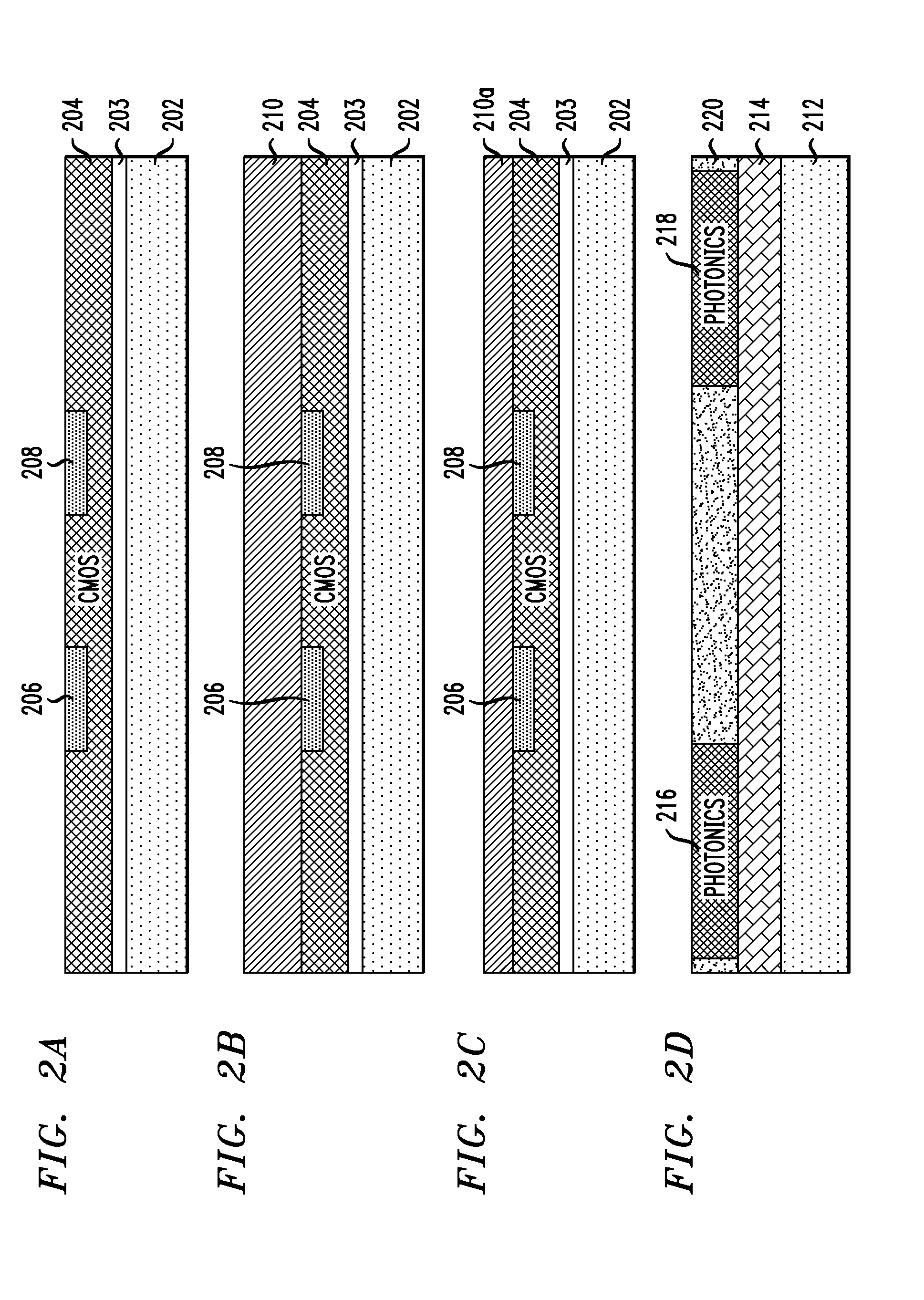
[0016]FIG. 1 is a diagram illustrating exemplary methodology 100 for fabricating a three-dimensional integrated circuit. Specifically, FIG. 1 provides an overview of a process whereby analog complementary metal-oxide semiconductor (CMOS) and photonics components (also referred to herein collectively as “analog CMOS / photonics circuitry”), fabricated on a common silicon-on-insulator (SOI) top wafer, are integrated with digital CMOS components (also referred to herein collectively as “digital CMOS circuitry”) fabricated on a common SOI or bulk-silicon (Si) bottom wafer. The designations “top” and “bottom” refer to an orientation of the wafers / device layers (see below) relative to one another in the fabricated circuit, and will be used to identify the wafers / device layers throughout the fabrication process. Further, the top wafer with analog CMOS / photonics circuitry and related components / layers is referred to hereinafter as a “top device layer,” and the bottom wafer with digital CMOS c...
PUM
 Abstract
Description
Claims
Application Information