Organic light emitting diode and method of fabricating the same

a light-emitting diode and organic technology, applied in the field of organic light-emitting diodes, can solve the problems of difficult limit of selection of auxiliary dopants, etc., and achieve the effect of improving the life of the device and facilitating the control of color coordinates

Active Publication Date: 2009-12-10
SAMSUNG DISPLAY CO LTD
View PDF5 Cites 37 Cited by
  • Summary
  • Abstract
  • Description
  • Claims
  • Application Information

AI Technical Summary

Benefits of technology

[0009]Aspects of the present embodiments provide an organic light emitting diode which can facilit...

Problems solved by technology

However, when the energy level of the auxiliary dopant is limited in that of the host, there is a limit to selection of the auxiliary dopant.
In addition, it is difficult to contr...

Method used


Image

  • Organic light emitting diode and method of fabricating the same
  • Organic light emitting diode and method of fabricating the same
  • Organic light emitting diode and method of fabricating the same

Examples


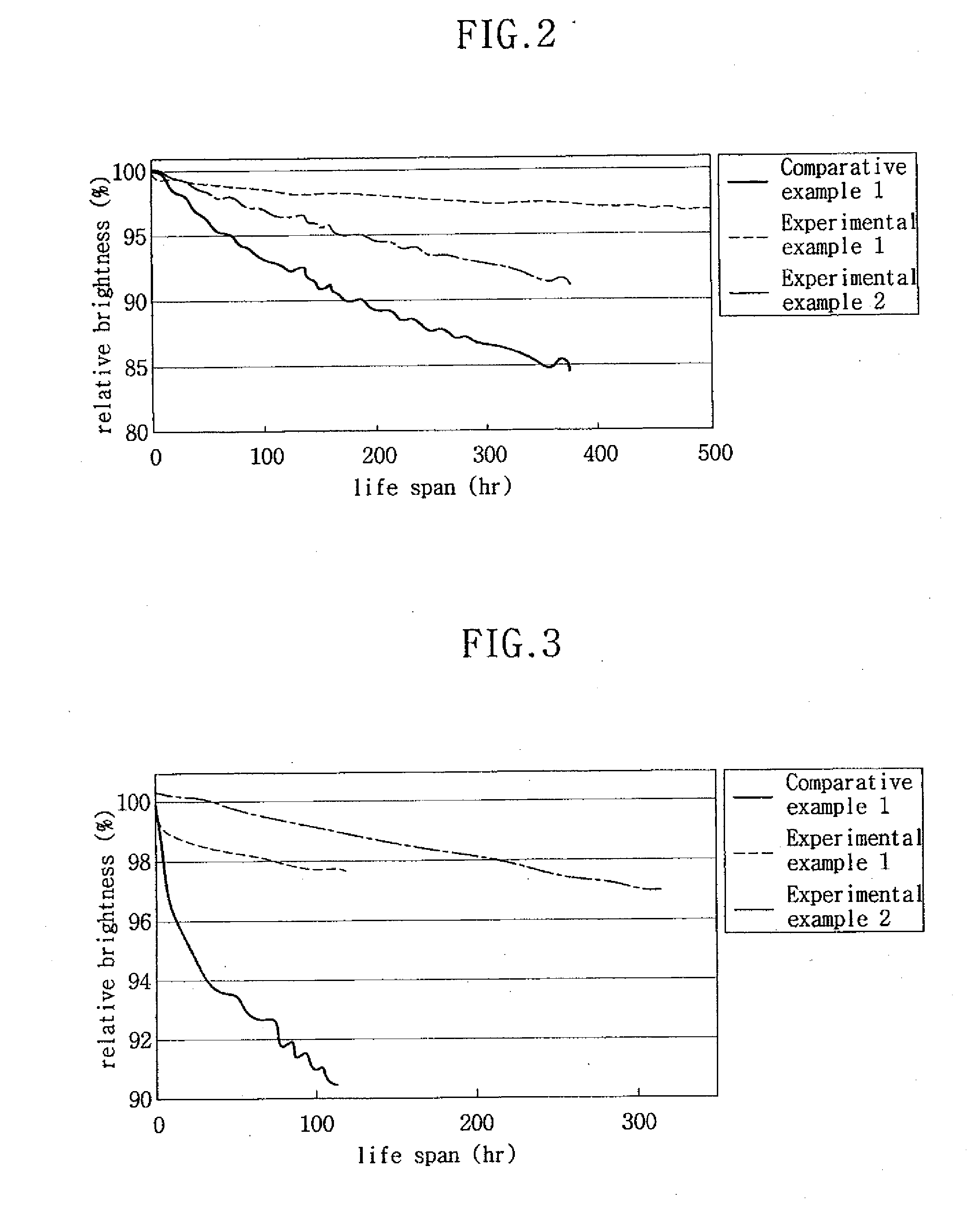
experimental example 1

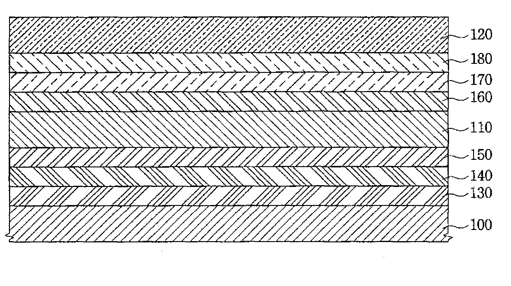
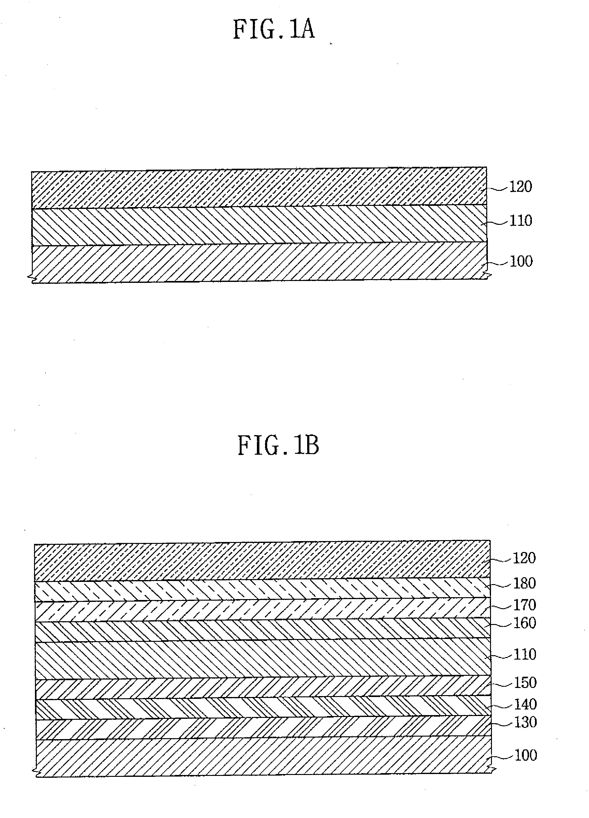
[0035]A first electrode was formed to a thickness of 1000 Å using indium tin oxide (ITO). Subsequently, a hole transport layer was formed to a thickness of 1000 Å using NPB on the first electrode. A red emission layer including rubrene as a host, 0.3 wt % RD3

(Kodak) as an emitting dopant, and 0.3 wt % as an auxiliary dopant was formed on the hole transport layer. The emission layer was formed to a thickness of 400 Å. An electron transport layer was formed to a thickness of 250 Å using TYE 704 (Toyo Ink Mfg. Co. Ltd., Tokyo, Japan) on the emission layer. An electron injection layer was formed to a thickness of 50 Å using LiF on the electron transport layer. A second electrode was formed to a thickness of 1500 Å using Al on the electron injection layer.

experimental example 2

[0036]The process described above for Experimental Example 1 was carried out

except that was included in the emission layer as an auxiliary dopant.

experimental example 3

[0041]A first electrode was formed to a thickness of 1000 Å using ITO. Subsequently, a hole transport layer was formed to a thickness of 1000 Å using NPB on the first electrode. A red emission layer was formed by stacking a 400 Å-thick first layer including rubrene as a host and 0.3 wt % RD3 (Kodak) as an emitting dopant on the hole transport layer, and a 150 Å-thick second layer including the host, the emitting dopant and

0.3 wt % as an auxiliary dopant on the first layer. An electron transport layer was formed to a thickness of 250 Å using TYE 704 (Toyo Ink) on the emission layer. An electron injection layer was formed to a thickness of 50 Å using LiF on the electron transport layer. A second electrode was formed to a thickness of 1500 Å using Al on the electron injection layer.


PUM


Abstract

Provided is an organic light emitting diode which can easily control color coordinates and improve a device's life span characteristic by using an auxiliary dopant having a higher band gap energy than that of a host, and preferably, having an absolute value of the highest occupied molecular orbital energy level equal to or higher than that of the host, or an absolute value of the lowest unoccupied molecular orbital energy level equal to or lower than that of the host.
The organic light emitting diode includes a first electrode, an emission layer disposed on the first electrode and including a host, an emitting dopant and an auxiliary dopant, and a second electrode disposed on the emission layer. Here, the auxiliary dopant has a higher band gap energy than the host. A method of fabricating the organic light emitting diode is provided.

Description

CROSS-REFERENCE TO RELATED APPLICATION[0001]This application claims the benefit of Korean Patent Application No. 10-2008-54283, filed Jun. 10, 2008, the disclosure of which is hereby incorporated herein by reference in its entirety.BACKGROUND OF THE INVENTION[0002]1. Field of the Invention[0003]The present embodiments relate to an organic light emitting diode (OLED) and a method of fabricating the same. Some embodiments relate to an OLED which uses an auxiliary dopant having a higher band gap energy than a host of an emission layer, and preferably having an absolute value of the highest occupied molecular orbital energy level equal to or higher than that of the host, or an absolute value of the lowest unoccupied molecular orbital energy level equal to or lower than that of the host, and thus can facilitate the control of color coordinates, and improve a device's life span, and a method of fabricating the same.[0004]2. Description of the Related Art[0005]Organic light emitting diodes...

Claims


Application Information

Patent Timeline
IPC IPC(8): H01L51/52H01L51/56
CPCH01L51/5012H01L51/56H01L51/5024H01L2251/552H10K50/11H10K2101/30H05B33/18H05B33/14H10K50/00H10K50/12H10K71/00
Inventor CHOI, SUNG-JINSONG, OK-KEUNJEONG, HYE-INKOO, YOUNG-MOLEE, MIN-WOO
Owner SAMSUNG DISPLAY CO LTD
Why Eureka
Try Eureka