Method and apparatus for flatband voltage tuning of high-k field effect transistors

a field effect transistor and flatband voltage technology, applied in the field of high-k field effect transistors, can solve the problems of difficult control of the flatband voltage of high-k based p n-type field effect transistors, inability to work, and large deviation of threshold voltage shifts

Active Publication Date: 2009-12-10
GLOBALFOUNDRIES US INC
View PDF14 Cites 5 Cited by
  • Summary
  • Abstract
  • Description
  • Claims
  • Application Information

AI Technical Summary

Problems solved by technology

Flatband voltages of high-k based p-type field effect transistors (pFETs) and n-type field effect transistors (nFETs) are difficult to control.
In some cases, electrode stacks are chosen according to workfunction to provide the desired flatbands, but this often does not work.
Moreover, threshold voltage shifts can vary significantly from desired values, and the causes for such shifts, which may be numerous, are not fully understood.

Method used


Image

  • Method and apparatus for flatband voltage tuning of high-k field effect transistors
  • Method and apparatus for flatband voltage tuning of high-k field effect transistors
  • Method and apparatus for flatband voltage tuning of high-k field effect transistors

Examples


first embodiment

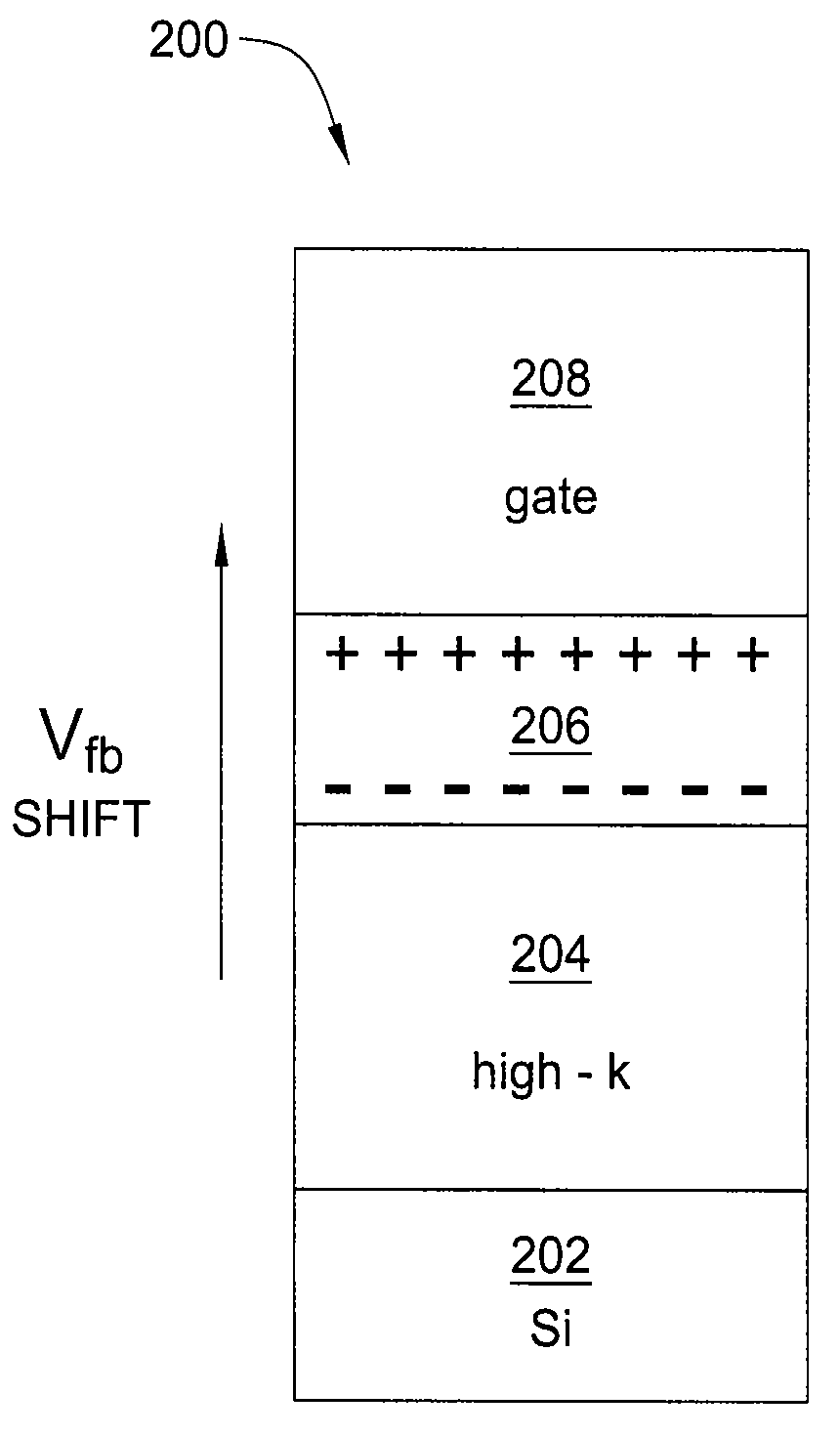
[0010]FIG. 1 is a schematic diagram illustrating a field effect transistor (FET) component 100 of a complementary metal-oxide-semiconductor (CMOS) device, fabricated in accordance with the present invention. Specifically, the FET 100 is an nFET.

[0011]The FET 100 comprises a silicon substrate layer 102, a high-k dielectric layer 104, a dipole layer 106, and a gate electrode 108.

[0012]In one embodiment, the silicon substrate layer 102 includes a chemical oxidation (CHEMOX) layer deposited thereon. In one embodiment, the CHEMOX layer has a thickness of approximately 0.5 nm.

[0013]The high-k dielectric layer 104 is deposited on the silicon substrate layer 102. In one embodiment, the high-k dielectric layer 104 comprises hafnium oxide (HfO2) or hafnium silicate (HfSiO). In one embodiment, the high-k dielectric layer 104 has a thickness of approximately two to approximately three nm.

[0014]The dipole layer 106 is deposited on the high-k dielectric layer 104. In one embodiment, the dipole la...

second embodiment

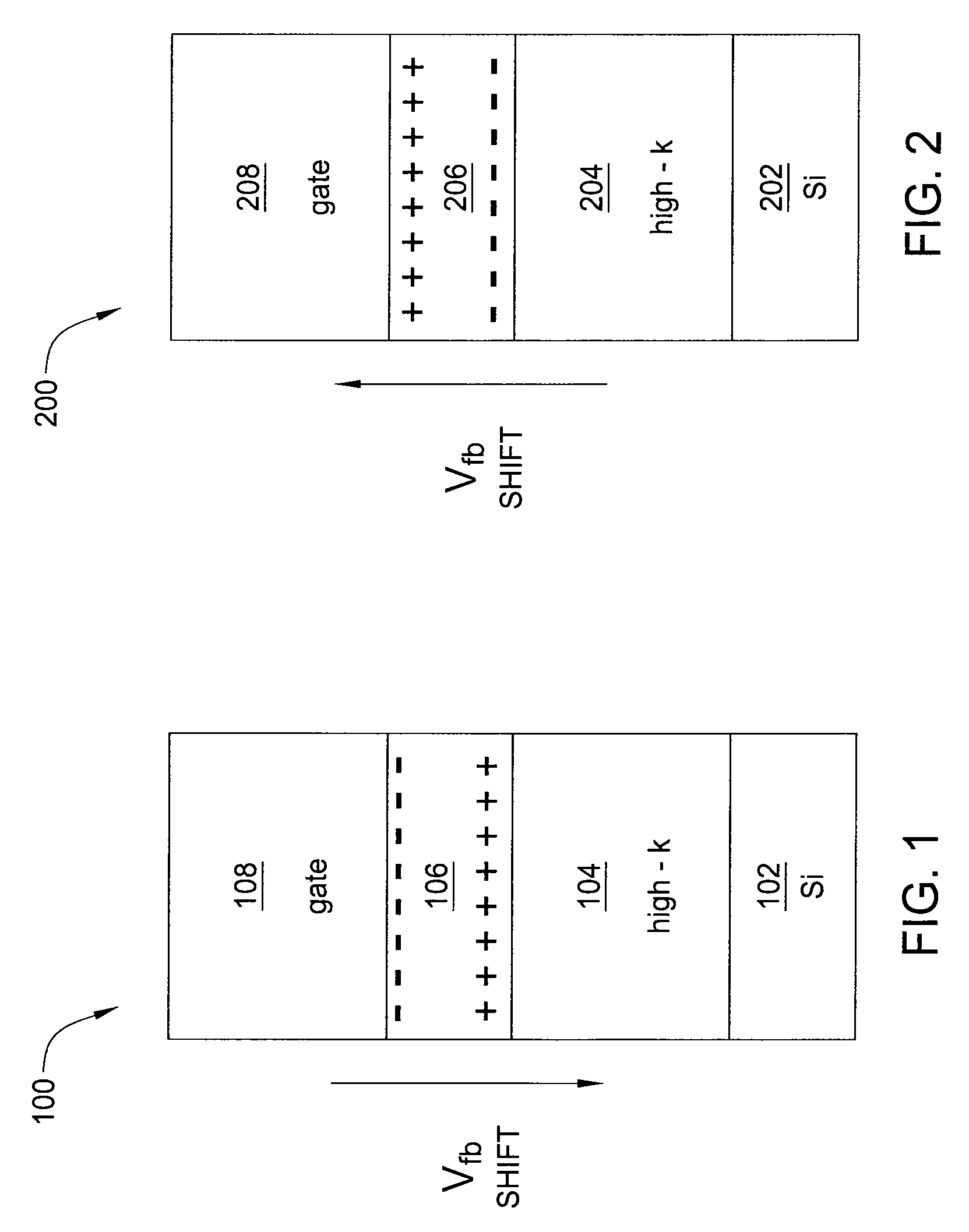
[0019]FIG. 2 is a schematic diagram illustrating a field effect transistor (FET) component 200 of a complementary metal-oxide-semiconductor (CMOS) device, fabricated in accordance with the present invention. Specifically, the FET 200 is a pFET.

[0020]The FET 200 comprises a silicon substrate layer 202, a high-k dielectric layer 204, a dipole layer 206, and a gate electrode 208.

[0021]In one embodiment, the silicon substrate layer 202 includes a chemical oxidation (CHEMOX) layer deposited thereon. In one embodiment, the CHEMOX layer has a thickness of approximately 0.5 nm.

[0022]The high-k dielectric layer 204 is deposited on the silicon substrate layer 202. In one embodiment, the high-k dielectric layer 204 comprises hafnium oxide (HfO2) or hafnium silicate (HfSiO). In one embodiment, the high-k dielectric layer 204 has a thickness of approximately two to approximately three nm.

[0023]The dipole layer 206 is deposited on the high-k dielectric layer 204. In one embodiment, the dipole lay...


PUM


Abstract

In one embodiment, the invention is a method and apparatus for flatband voltage tuning of high-k field effect transistors. One embodiment of a field effect transistor includes a substrate, a high-k dielectric layer deposited on the substrate, a gate electrode deposited on the high-k dielectric layer, and a dipole layer positioned between the substrate and the gate electrode, for shifting the threshold voltage of the field effect transistor.

Description

BACKGROUND OF THE INVENTION[0001]The present invention relates generally to high-k field effect transistors, and relates more particularly to flatband voltage tuning of high-k field effect transistors.[0002]Flatband voltage is the voltage at which there is no electrical charge in a semiconductor and, therefore, no voltage drop across the semiconductor (i.e., in a band diagram the energy bands of the semiconductor are horizontal (flat)). Flatband voltages of high-k based p-type field effect transistors (pFETs) and n-type field effect transistors (nFETs) are difficult to control.[0003]For instance, in conventional metal-oxide-semiconductor FETs (MOSFETs), the threshold voltage often fails to meet the desired value (e.g., +0.3 V for both pFETs and nFETs). In some cases, electrode stacks are chosen according to workfunction to provide the desired flatbands, but this often does not work. Moreover, threshold voltage shifts can vary significantly from desired values, and the causes for suc...

Claims


Application Information

Patent Timeline
Patent Type & Authority Applications(United States)
IPC IPC(8): H01L29/78H01L21/3205
CPCH01L21/28088H01L21/28194H01L29/517H01L29/513H01L29/4966
Inventor GUHA, SUPRATIKNARAYANAN, VIJAYPARUCHURI, VAMSI K.
Owner GLOBALFOUNDRIES US INC
Why Eureka
Try Eureka