Optical filtering matrix structure and associated image sensor

Inactive Publication Date: 2009-12-10
COMMISSARIAT A LENERGIE ATOMIQUE ET AUX ENERGIES ALTERNATIVES
View PDF6 Cites 53 Cited by
  • Summary
  • Abstract
  • Description
  • Claims
  • Application Information

AI Technical Summary

Problems solved by technology

One of the important problems to be solved for an image sensor is that of obtaining colors.
A drawback of this sensor however is its impossibility of filtering infrared.
This pixel size then poses a problem when the rays arrive with strong incidence at the surface of the sensor (image edge or strongly open objective).
This phenomenon therefore consi

Method used


Image

  • Optical filtering matrix structure and associated image sensor
  • Optical filtering matrix structure and associated image sensor
  • Optical filtering matrix structure and associated image sensor

Examples


first embodiment

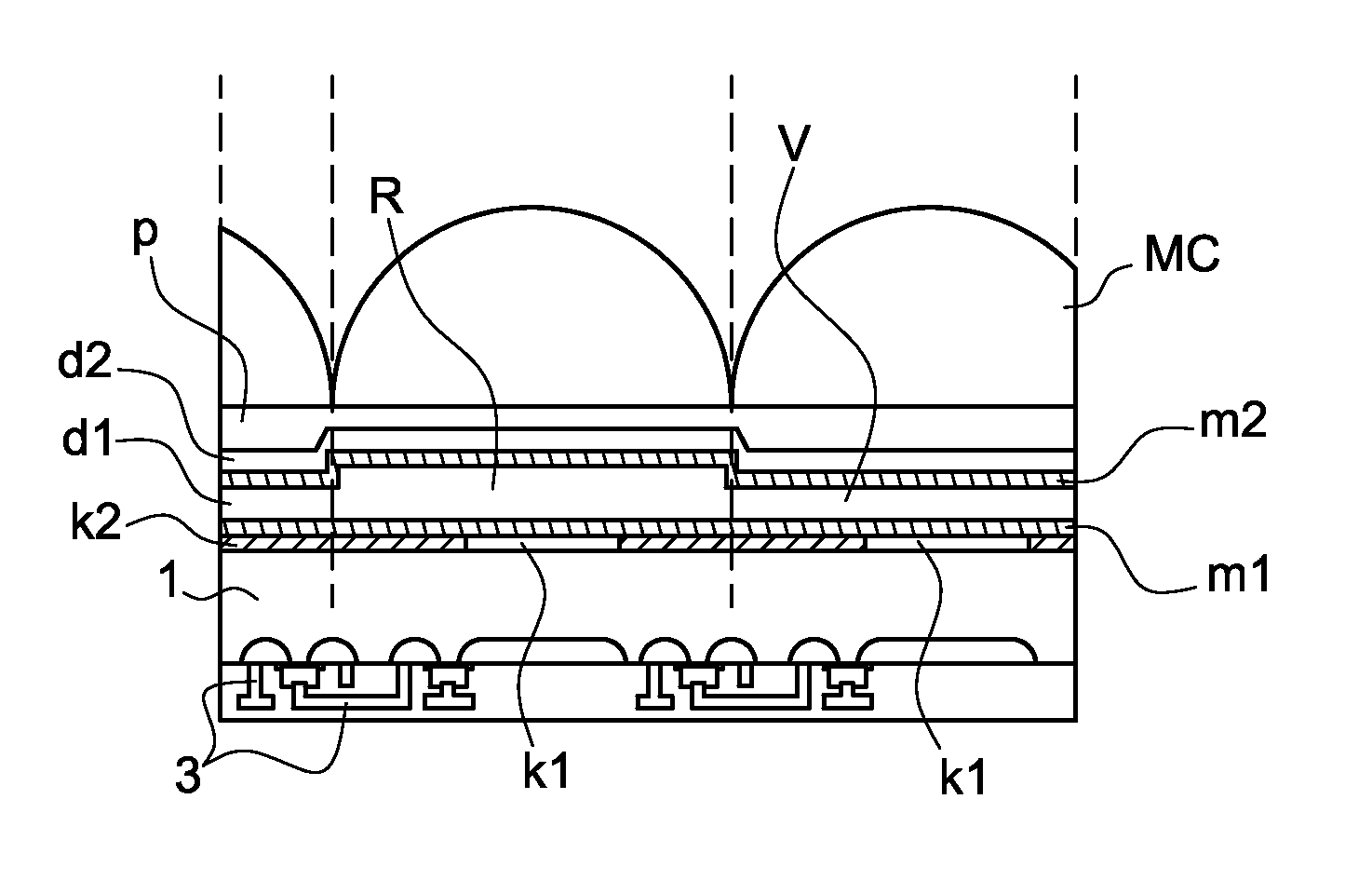
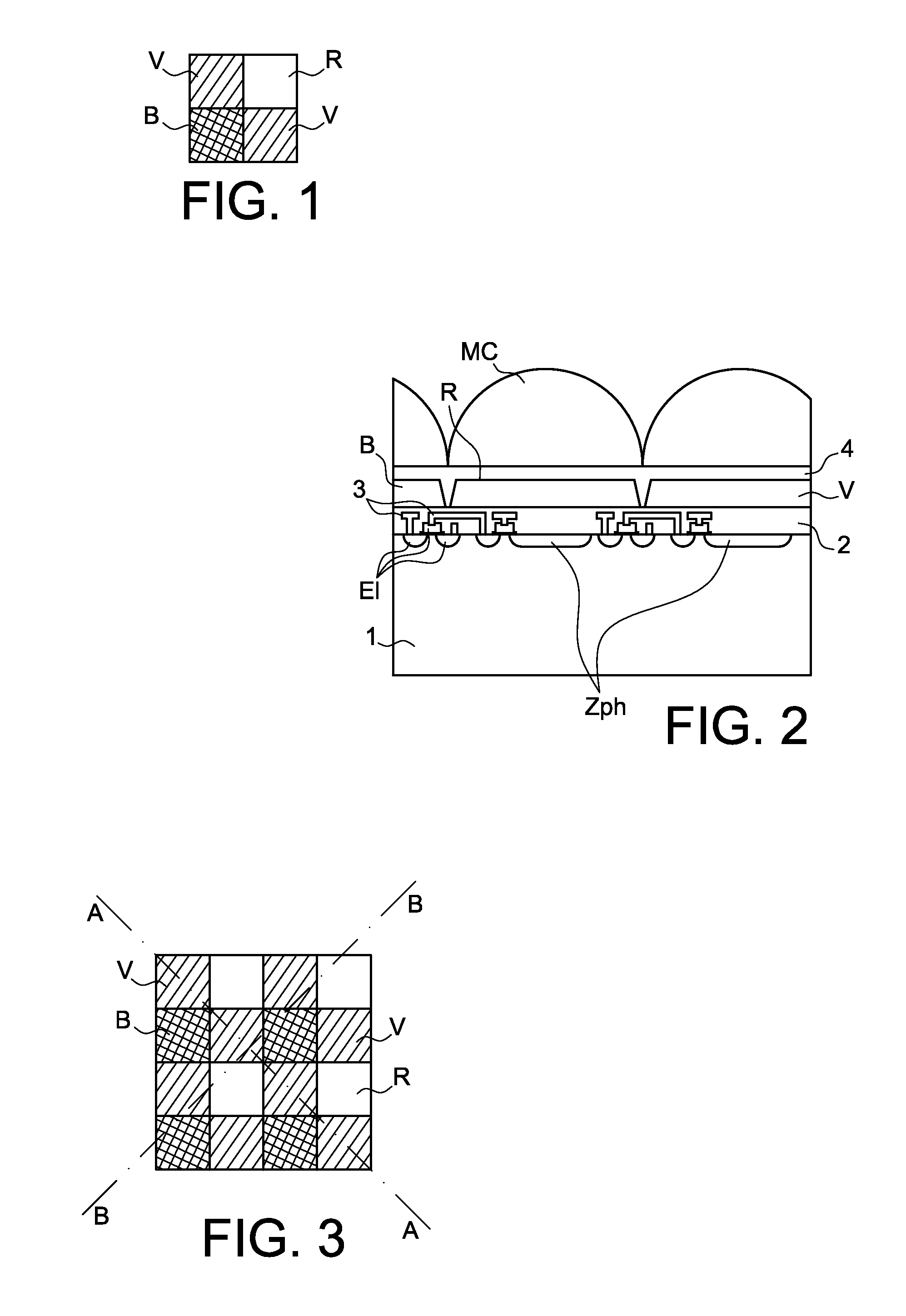
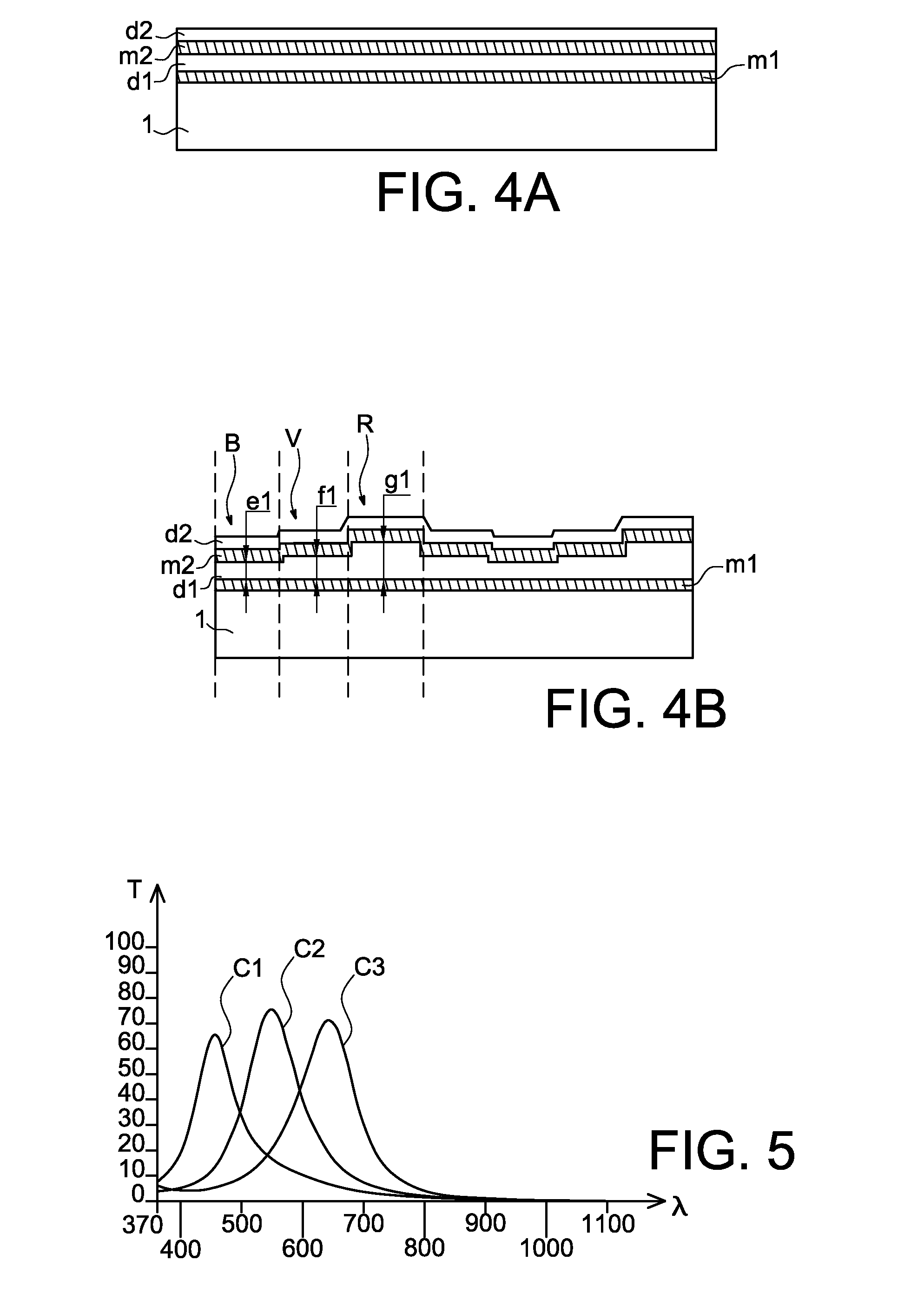
[0049]FIGS. 4A and 4B illustrate sectional views, along two different axes, of an optical filtering matrix structure according to the invention. With reference to FIG. 3, FIG. 4A is a sectional view along the axis AA of FIG. 3 and FIG. 4B is the sectional view along the axis BB of FIG. 3. The AA axis diagonally cuts the green optical filters V. The BB axis is an axis perpendicular to the AA axis and cuts, outside the diagonals, successive blue B, green V, red R, green V, blue B, green V, red R, etc. optical filters.

[0050]The image sensor comprises a photosensitive semiconducting element 1, for example silicon, on which a first metal layer m1, a first transparent layer d1, a second metal layer m2 and a second transparent layer d2 are successively laid. The metal used for producing the metal layers m1 and m2 is silver (Ag) for example and the material used for producing the transparent layers d1 and d2 is a dielectric for example, which may be titanium dioxide (TiO2) for example.

[0051...

second embodiment

[0058]FIGS. 6A and 6B illustrate sectional views, along two different axes of an optical filtering matrix structure according to the invention. With reference to FIG. 3, FIG. 6A is a sectional view along the AA axis and FIG. 6B is a sectional view along the BB axis.

[0059]The image sensor comprises a photosensitive semiconducting element 1, for example silicon, on which three metal layers m1, m2, m3 and three transparent layers d1, d2, d3 are alternately laid, the metal layer m1 being in contact with the semiconducting element 1. The metal layers m1-m3 are in silver (Ag) for example, and the transparent layers d1-d3 are in titanium dioxide (TiO2) for example.

[0060]The layers d1 and d2 are adjustment layers, of which the changes in thickness set the different transmission wavelengths of the filter, all the other layers having a constant thickness. An overthickness resulting from a change in thickness of the layer d1 coincides with an overthickness resulting from a change in thickness ...


PUM


Abstract

The invention relates to an optical filtering structure consisting of a set of at least two elementary optical filters (R, V, B), an elementary optical filter being centered on an optimum transmission frequency, characterized in that it comprises a stack of n metal layers (m1, m2, m3) and n substantially transparent layers (d1, d2, d3) which alternate between a first metal layer (m1) and an nth substantially transparent layer (d3), the n metal layers (m1, m2, m3) each having a constant thickness and at least one substantially transparent layer having a variable thickness which sets the optimum transmission frequency of an elementary optical filter, n being an integer larger than or equal to 2.

Description

TECHNICAL FIELD AND PRIOR ART[0001]The invention relates to an optical filtering matrix structure and an image sensor which comprises an optical filtering matrix structure according to the invention.[0002]The invention finds a particular advantageous application for producing image sensors of small dimensions such as for example, miniature camera image sensors of mobile telephones.[0003]Obtaining images by an electronic sensor is in full development. The demand for simplification of the production of the sensors continues to be very strong. Charge coupled devices, more commonly called CCD sensors, are gradually replaced with active pixel sensors in CMOS technology, more commonly called CMOS APS (Active Pixel Sensor) sensors.[0004]One of the important problems to be solved for an image sensor is that of obtaining colors. It is known that starting with three colors taken from the visible spectrum (red, green, blue), it is possible to record and to then reproduce the majority of colors...

Claims


Application Information

Patent Timeline
IPC IPC(8): H01L31/0232G02B5/28
CPCG02B5/201H01L27/14609G02B5/288H01L27/14627H01L27/14632H01L27/14621G02B5/20H01L27/146H01L31/0216
Inventor GIDON, PIERREGRAND, GILLES
Owner COMMISSARIAT A LENERGIE ATOMIQUE ET AUX ENERGIES ALTERNATIVES
Why Eureka
Try Eureka