

Laminate substrate and semiconductor package utilizing the substrate
a technology of laminate substrate and semiconductor package, which is applied in the direction of printed circuit, printed circuit components, printed circuit stress/warp reduction, etc., can solve the problems of substrate warpage, difficult packaging process, warpage and deformation, etc., and achieve the effect of suppressing substrate warpage, reducing the manufacturing cost of the substrate, and suppressing the warpage of the substra
- Summary
- Abstract
- Description
- Claims
- Application Information
AI Technical Summary
Benefits of technology
Problems solved by technology
Method used
Image

Examples
Embodiment Construction
[0013]Please refer to the attached drawings, the present invention are described by means of embodiments below.
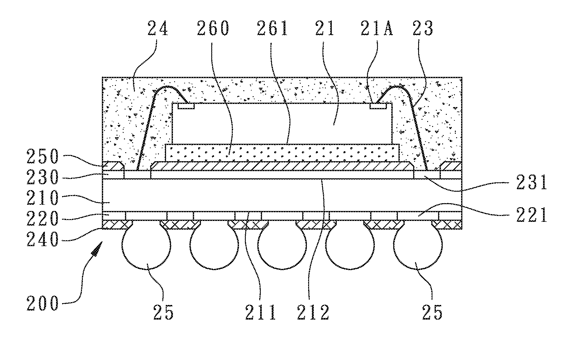
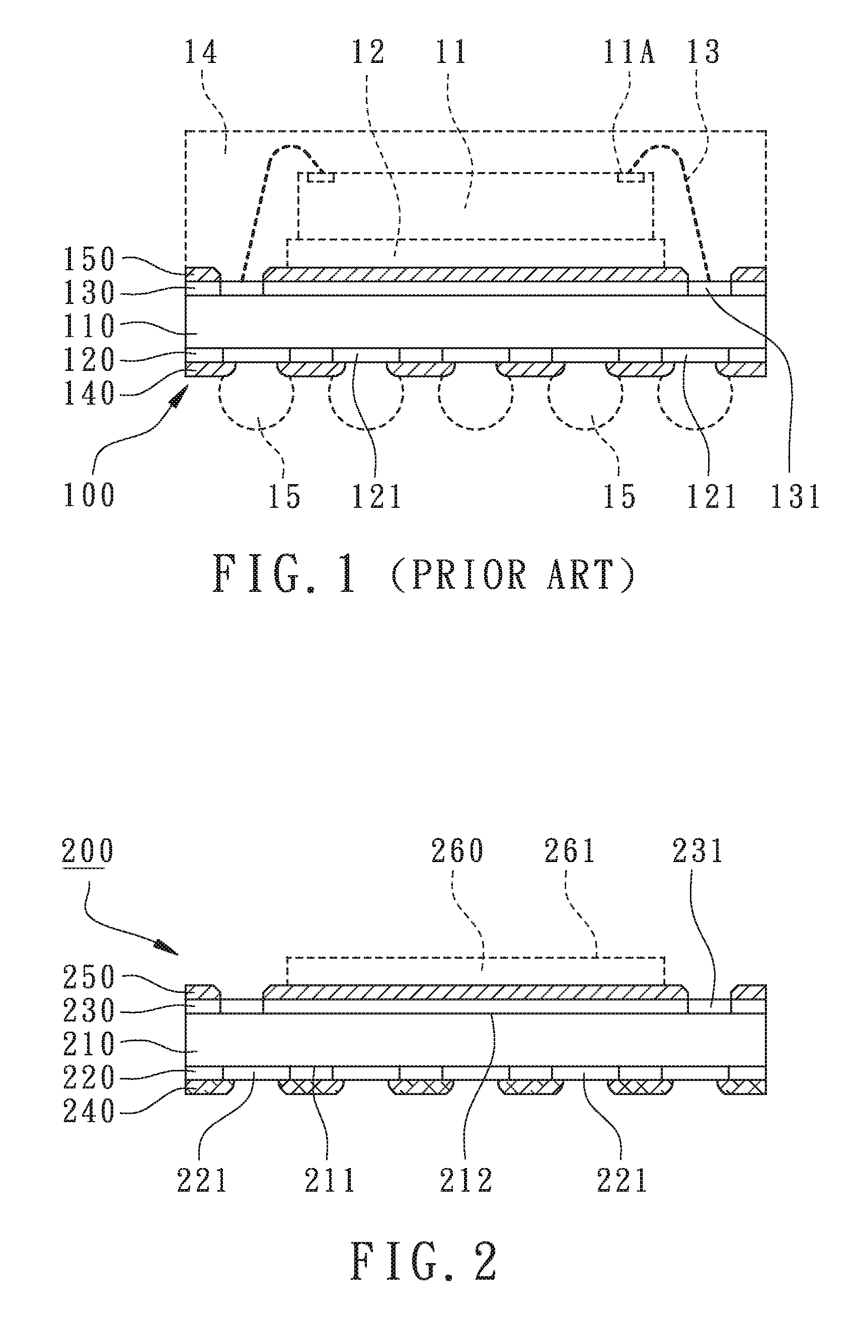
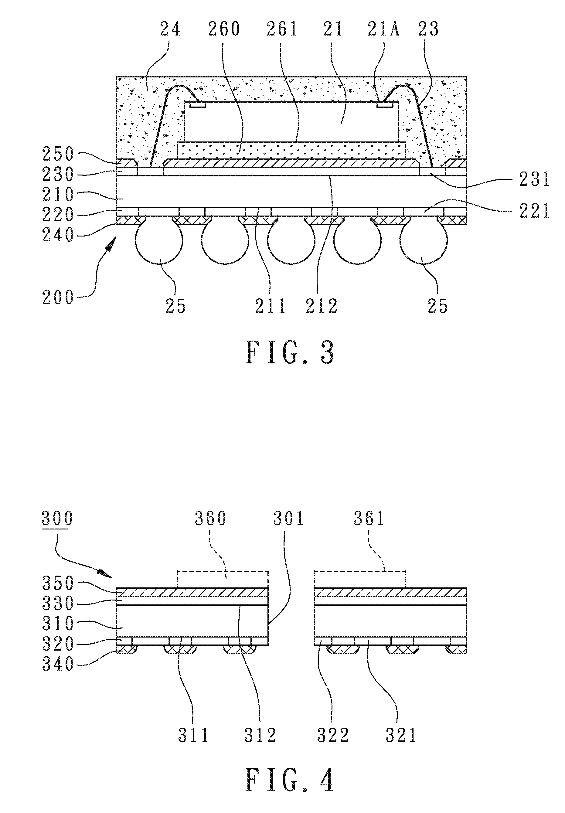
[0014]A laminated substrate according to the first embodiment of the present invention is illustrated in the cross-sectional view of FIG. 2. The laminated substrate 200 comprises a core layer 210, a first metal layer 220, a second metal layer 230, a first solder mask 240, and a second solder mask 250. The core layer 210 has a first surface 211 and a second surface 212. In the manufacturing processes of a laminated substrate, the core layer 210 is the base layer where the metal layers 220 and 230 and the solder masks 240 and 250 are sequentially disposed on the surfaces of the core layer 210. In other embodiments, the internal stacked layers or external added layers can be appropriately adjusted for easy trace layouts. The core layer 210 is the intermediate layer of the substrate 200 which includes glass fibers mixed with resins where the resin is chosen from epoxy resin, po...
PUM
| Property | Measurement | Unit |
|---|---|---|
| thicknesses | aaaaa | aaaaa |
| CTE | aaaaa | aaaaa |
| density | aaaaa | aaaaa |
Abstract
Description
Claims
Application Information