On-Chip Source Termination in Communication Systems

a source termination and communication system technology, applied in the field of communication systems, can solve the problems of reducing the return loss performance of off-chip source terminations at higher frequencies, affecting the matching of source impedances, and reducing voltage peaking and/or voltage overshoo

Inactive Publication Date: 2009-12-10
AVAGO TECH INT SALES PTE LTD
View PDF26 Cites 1 Cited by
  • Summary
  • Abstract
  • Description
  • Claims
  • Application Information

AI Technical Summary

Benefits of technology

[0009]The present invention provides an integrated circuit (IC) chip that includes an on-chip source termination. The on-chip source termination can be a non-precision resistor, such as an unsilicided poly resistor, or any other suitable termination. The on-chip source termination can facilitate matching a source impedance of the IC chip and a load impedance of a load connected to the IC chip. The on-chip source termination can absorb reflections on a transmission line to which the IC chip is connected. As compared to an off-chip source termination, the on-chip source termination can reduce voltage peaking and / or voltage overshoot in the IC die and / or at the load that is connected to the IC chip.

Problems solved by technology

Parasitics between the chip and the off-chip source termination can cause hybrid residual for bi-directional communication systems.
Off-chip source terminations can cause voltage peaking or voltage overshoot inside the transmitter and / or at the load.
The return loss performance of off-chip source terminations degrades substantially at higher frequencies.

Method used


Image

  • On-Chip Source Termination in Communication Systems
  • On-Chip Source Termination in Communication Systems
  • On-Chip Source Termination in Communication Systems

Examples


Embodiment Construction

[0037]Although the embodiments of the invention described herein refer specifically, and by way of example, to Ethernet systems, including Ethernet transmitters, it will be readily apparent to persons skilled in the relevant art(s) that the invention is equally applicable to other communication systems, including but not limited to serializer / deserializer (SerDes) systems, optical systems, cable systems, digital subscriber line (DSL) systems, and / or any combination thereof. An Ethernet transmitter can be an Ethernet transceiver, for example. It will also be readily apparent to persons skilled in the relevant art(s) that the invention is applicable to any communication system requiring an accurate transmit voltage.

1.0 Integrated Circuit (IC) Package

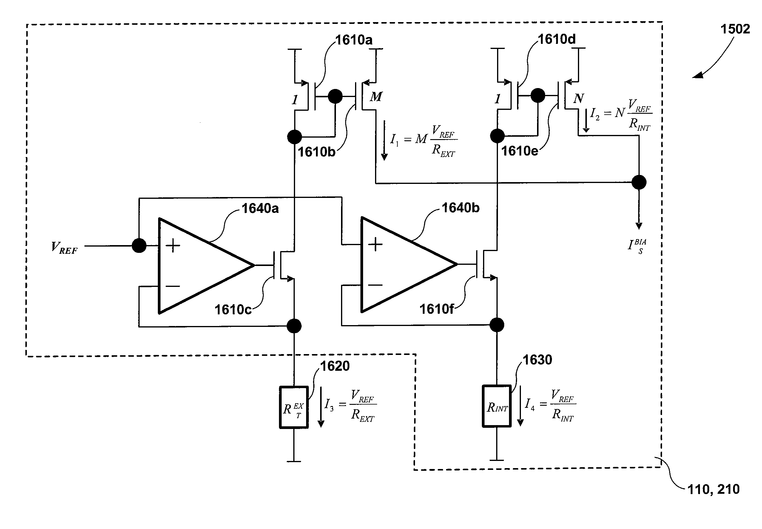
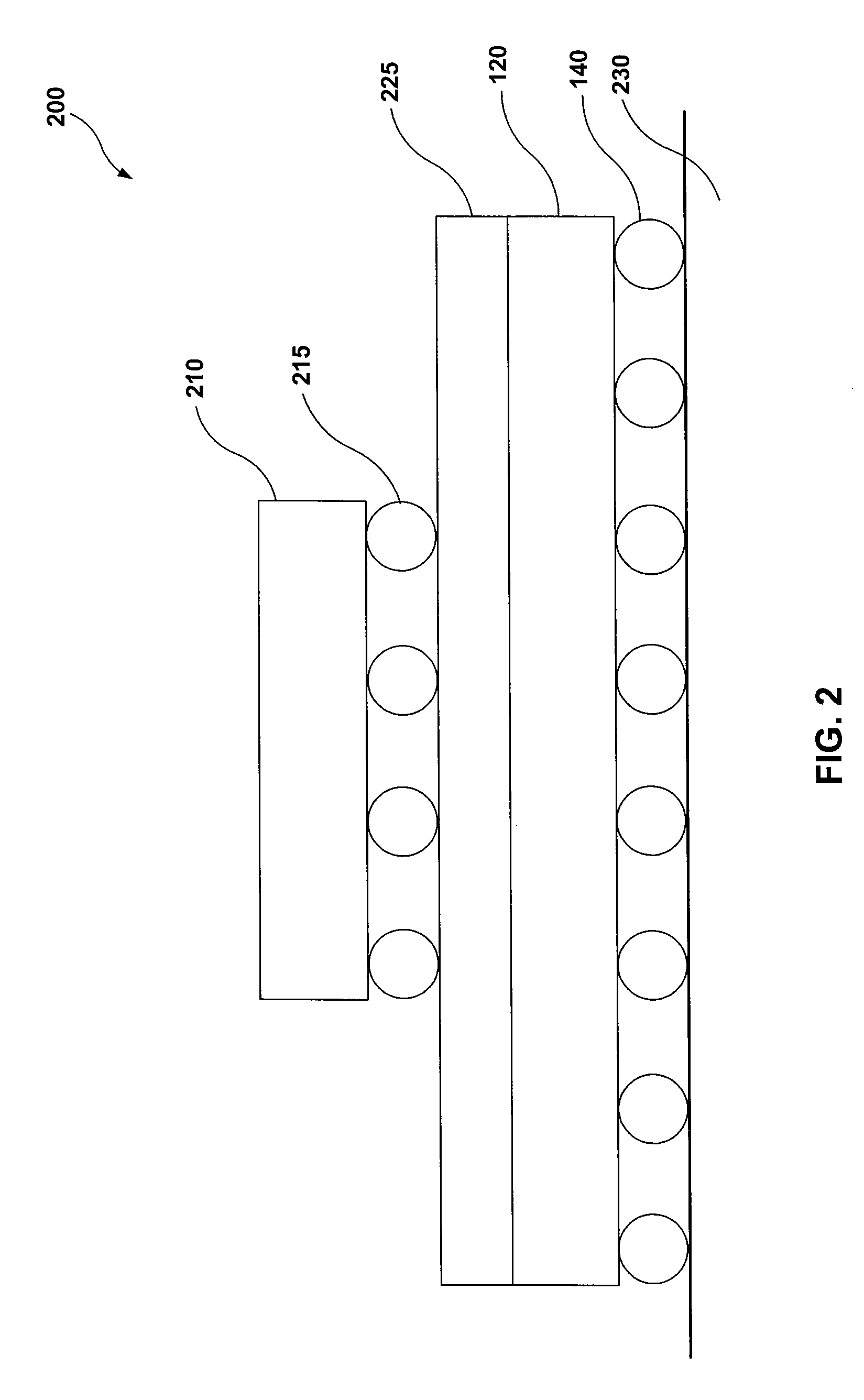
[0038]FIG. 1 illustrates an integrated circuit (IC) package 100 according to an embodiment of the present invention. The IC package 100 includes an IC die 110, bond wires 115, and a substrate 120. IC die 110 can be coupled to substrate 120...


PUM


Abstract

An apparatus and system are provided to adjust an output voltage of an integrated circuit (IC) die. For instance, the apparatus can include an on-chip source termination and a bias generator. The bias generator can be configured to provide a source current to the on-chip source termination to adjust the output voltage. In particular, when adjusting the output voltage of the IC die, the bias generator can adjust the source current using a first current with a first adjustable current gain and a second current source with a second adjustable current gain.

Description

CROSS REFERENCE TO RELATED APPLICATIONS[0001]This application is a continuation of U.S. patent application Ser. No. 11 / 980,541, “On-Chip Source Termination in Communication Systems,” filed Oct. 31, 2007, now allowed, which is a divisional of U.S. patent application Ser. No. 11 / 115,117, “On-Chip Source Termination in Communication Systems,” filed Apr. 27, 2005, U.S. Pat. No. 7,301,365, which are both incorporated by reference herein in their entireties.BACKGROUND[0002]1. Field[0003]The present invention relates generally to communication systems, and more specifically to source termination in communication systems.[0004]2. Background[0005]Devices in a communication system generally include transmitters to transmit information via an electrically conductive medium, such as a transmission line. For instance, a transmitter in a first device can transmit information to a receiver in a second device, and a transmitter in the second device can transmit information to a receiver in the firs...

Claims


Application Information

Patent Timeline
Patent Type & Authority Applications(United States)
IPC IPC(8): H03K17/16H03K17/30
CPCH04L25/0298
Inventor CHAN, KEVIN T.
Owner AVAGO TECH INT SALES PTE LTD
Why Eureka
Try Eureka