
Image Display Device

a display device and image technology, applied in the direction of static indicating devices, instruments, etc., can solve the problems of not ensuring precise correction and creating brightness differences between adjacent pixels

Active Publication Date: 2009-12-10
SAMSUNG DISPLAY CO LTD +1
View PDF8 Cites 15 Cited by
  • Summary
  • Abstract
  • Description
  • Claims
  • Application Information

AI Technical Summary

Benefits of technology

[0016]The present invention has been made in view of the above-mentioned problems of prior art, and it is therefore an object of the present invention to provide a technology with which deterioration of a self-light-emitting element in an image display device can be corrected precisely.

Problems solved by technology

A part in which the white square is displayed deteriorates more quickly than a part in which black is displayed, thereby creating a difference in brightness between adjacent pixels.
The technologies described in JP 2005-156697 A and JP 2002-341825 A therefore do not ensure precise correction even when accurate detection operation is carried out.

Method used


Image

  • Image Display Device
  • Image Display Device
  • Image Display Device

Examples


Embodiment Construction

[0043]An embodiment of the present invention is described below in detail with reference to the accompanying drawings.

[0044]Components having the same functions are denoted by the same reference symbols throughout the drawings that illustrate the embodiment, and repetitive descriptions are omitted.

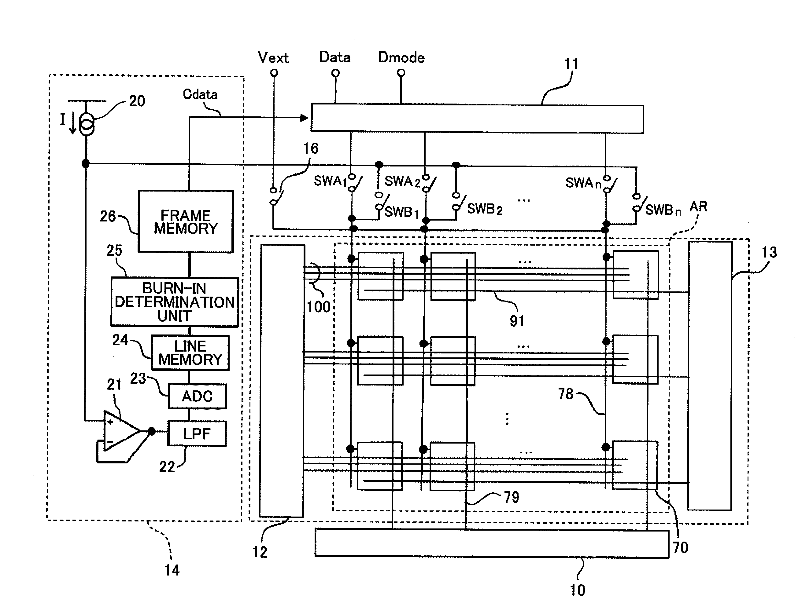
[0045]FIG. 1 is a diagram illustrating a schematic structure of an organic EL display panel with a built-in burn-in detection and correction function according to the embodiment of the present invention.

[0046]In this embodiment, as illustrated in FIG. 1, a characteristics detection unit 14 first causes a constant current to flow from a current source 20 into each organic EL element, and detects the resultant anode voltage of the organic EL element through a buffer circuit 21 and a low pass filter 22. An analog-digital conversion circuit 23 converts the detected anode voltage into a digital value, which is stored in a line memory 24.

[0047]From the information stored in the line memory 24, a...


PUM


Abstract

Provided is an image display device in which deterioration of a self-light-emitting element within a pixel is corrected accurately. A detection unit detects, within a detection period, a difference in characteristics between self-light-emitting elements of adjacent pixels. A first subtraction circuit outputs a differential voltage between a reference voltage and an image voltage to a self-light-emitting element that is determined by the detection unit as a deteriorated element. An amplifier amplifies an output of the first subtraction circuit with a gain [1 / {1-(α / 100)}]1 / 2 when a driver transistor is driven in a saturation region. The amplifier amplifies the output of the first subtraction circuit with a gain [1 / {1-(α / 100)}] when the driver transistor is driven in a linear region. A differential between the reference voltage and an output of the amplifier obtained by a second subtraction circuit is used as a corrected image voltage.

Description

CROSS-REFERENCE TO RELATED APPLICATION[0001]The present application claims priority from Japanese application JP 2008-146916 filed on Jun. 4, 2008, the content of which is hereby incorporated by reference into this application.BACKGROUND OF THE INVENTION[0002]1. Field of the Invention[0003]The present invention relates to an image display device, and more particularly, to an active matrix organic electroluminescence display.[0004]2. Description of the Related Art[0005]There are great expectations on organic electroluminescence displays (hereinafter referred to as organic EL display devices) which each include an organic electroluminescence display panel (hereinafter referred to as organic EL display panel) driven by active matrix driving, as flat panel displays of a next generation.[0006]The organic EL display panel usually includes an organic electroluminescence element (hereinafter referred to as organic EL element) and a driving-use thin film transistor for supplying a current to...

Claims


Application Information

Patent Timeline
Patent Type & Authority Applications(United States)
IPC IPC(8): G09G3/30
CPCG09G3/3225G09G3/3291G09G2300/0842G09G2300/0861G09G2320/046G09G2320/0285G09G2320/0295G09G2320/043G09G2320/0233
Inventor KOHNO, TOHRUAKIMOTO, HAJIMEKASAI, NARUHIKOISHII, MASATO
Owner SAMSUNG DISPLAY CO LTD
Features
  • Generate Ideas
  • Intellectual Property
  • Life Sciences
  • Materials
  • Tech Scout
  • Unparalleled Data Quality
  • Higher Quality Content
  • 60% Fewer Hallucinations
Learn More