Package substrate having double-sided circuits and fabrication method thereof

Inactive Publication Date: 2009-12-17
PHOENIX PRECISION TECH CORP
View PDF2 Cites 19 Cited by
  • Summary
  • Abstract
  • Description
  • Claims
  • Application Information

AI Technical Summary

Benefits of technology

[0020]Therefore, a package substrate having double-sided circuits and a fabrication method thereof are provided by the present invention by the design that a top surface of a plurality of first electrical contact pads is higher than the top surface of the first wiring layer. In contrast to prior art, the present invention provides a plurality of first electrical contact pads for replacing solder bumps so as to dispense with the solder bumps otherwise necessary for the prior art. Moreover, the average value

Problems solved by technology

However, as the number of layers of a multi-layer board increases, paths of electric current, and thickness of the substrate increase to the detriment of miniaturization and high-speed transmission.
With the solder bumps being formed by screen printing, the average allowable tolerance in volume and height of the solder bumps are difficult to control, Therefore, bonding of the first electrical contact pads 132a and the solder bumps is weak, which further affects electrical connection yield of the semiconductor chip.
For example, in case of great

Method used


Image

  • Package substrate having double-sided circuits and fabrication method thereof
  • Package substrate having double-sided circuits and fabrication method thereof
  • Package substrate having double-sided circuits and fabrication method thereof

Examples


Example

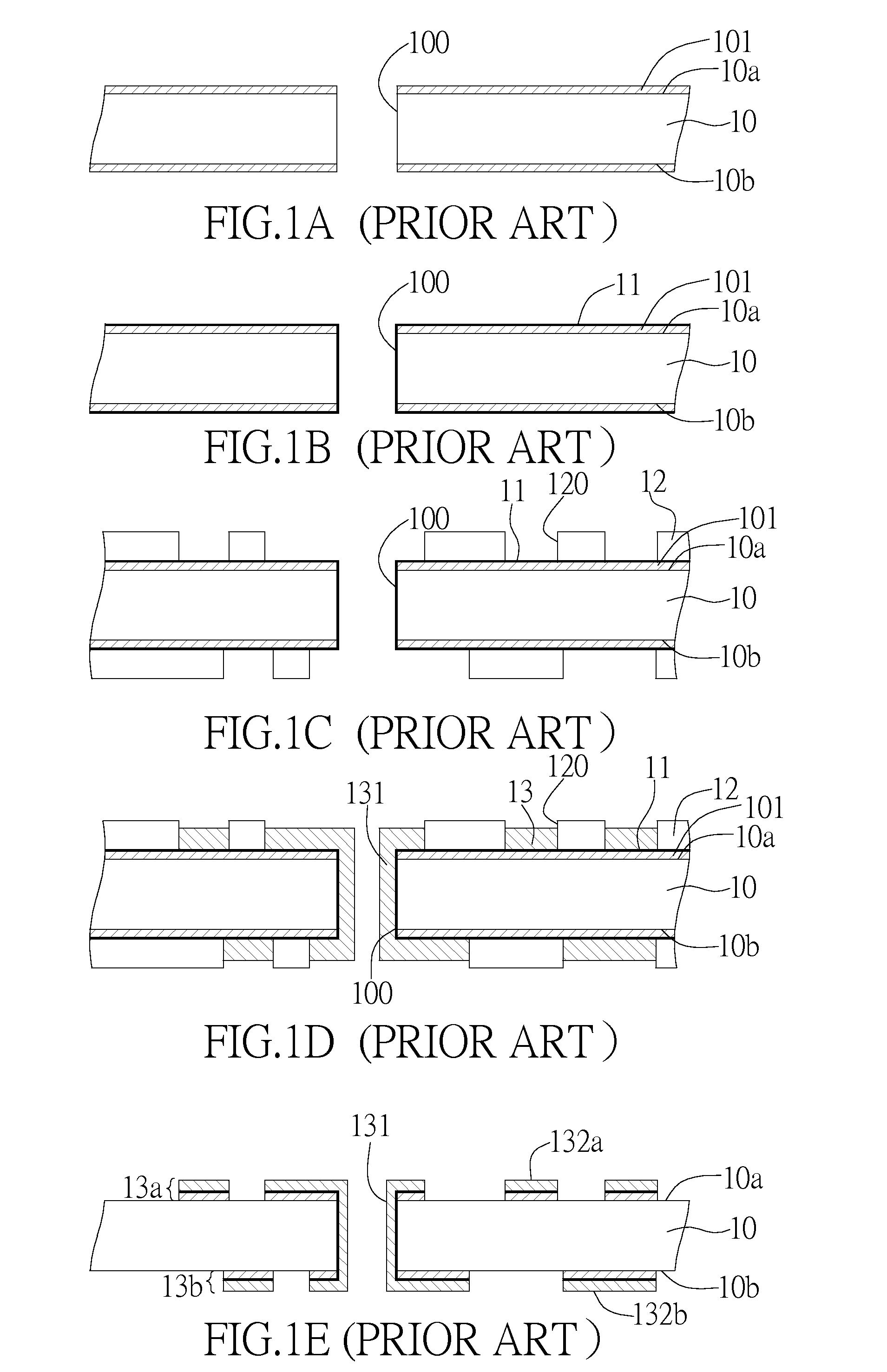
[0026]FIGS. 2A to 2K are cross-sectional diagrams showing a package substrate having double-sided circuits and a fabrication method thereof according to a first embodiment of the present invention.

[0027]Referring to FIG. 2A, a core board 20 which functions as an insulating board is provided, and the core board 20 has a first surface 20a and a second surface 20b opposing each other. As shown in the drawing, a first metallic layer 21 is formed on the first and second surfaces 20a, 20b, and a through-hole 200 is formed to penetrate the first metallic layer 21 and the first and second surfaces 20a, 20b.

[0028]Referring to FIG. 2B, a conductive layer 22 is formed on the first metallic layer 21 and walls of the through-hole 200. The conductive layer 22 is mainly used as a path of electric current required by a subsequent metal-plating process (to be described below). The conductive layer 22 is made of a metal or an alloy, or comprises a plurality of deposited metallic layer. For example, ...

Example

Second Embodiment

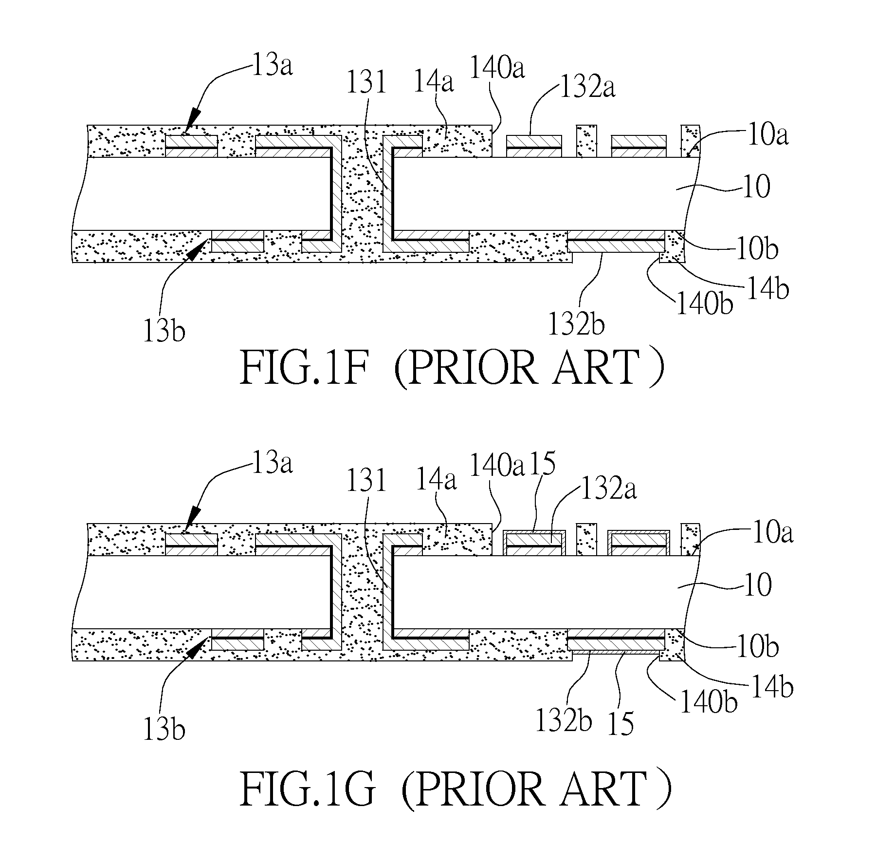
[0046]FIGS. 3A to 3H are cross-sectional diagrams showing a package substrate having double-sided circuits and a fabrication method thereof according to a second embodiment of the present invention. The present embodiment is substantially the same with the first embodiment except that, in the present embodiment, an etching stop layer protects a plated through hole.

[0047]Referring to FIG. 3A, a structure similar to one shown in FIG. 2D is provided. The second metallic layer 24 is formed in the first opening portions 230a of the first resist layer 23a by plating via the conductive layer 22. Further, the plated through hole 241 is formed in the through-hole 200 by plating a metallic material thereto, and the plated through hole 241 has the connection ring 242 extended to the first surface 20a and the second surface 20b; wherein the through-hole 200 is not fully filled with metal so that the plated through hole 241 is of a hollow shape.

[0048]Referring to FIG. 3B, a seco...

Example

Third Embodiment

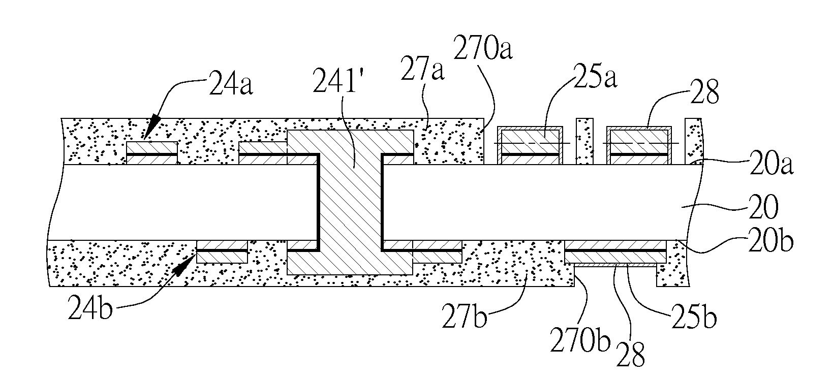
[0062]FIGS. 4A to 4H are cross-sectional diagrams showing a package substrate having double-sided circuits and a fabrication method thereof according to a third embodiment of the present invention. The present embodiment is substantially the same with the first and second embodiments except that, in the present embodiment, the plated through hole is of a solid shape and is filled with a metallic material by plating.

[0063]Referring to FIG. 4A, a structure similar to FIG. 2D is provided. The second metallic layer 24 is formed in the first opening portions 230a by plating. Further, the through-hole 200 is filled in full with metal by plating a metallic material to the through-hole 200, so that the plated through hole 241′ thus formed is of a solid shape. And the plated through hole 241′ is provided with the connection ring 242 on the first surface 20a and the second surface 20b.

[0064]Referring to FIG. 4B, the second resist layer 23b is formed on the second metallic lay...


PUM


Abstract

A package substrate having double-sided circuits and a method of manufacturing the same are proposed. The package substrate includes a core board having a plated through hole, a plurality of first electrical contact pads, and a first solder mask layer formed on the core board. A first wiring layer and a second wiring layer are disposed on two opposite surfaces of the core board, respectively, and electrically connected to the plated through hole. A portion of the first wiring layer is exposed from a first opening formed in the first solder mask layer. The first electrical contact pads are disposed on the exposed portion of the first wiring layer. The top surface of the first electrical contact pads is higher than that of the first wiring layer to thereby allow a semiconductor chip to be mounted on the electrical contact pads for improving electrical connection.

Description

FIELD OF THE INVENTION[0001]The present invention relates to package substrates, and more particularly, to a package substrate having double-sided circuits.DESCRIPTION OF RELATED ART[0002]In order to satisfy the requirements of high integration and miniaturization of the semiconductor package, multi-layer boards have emerged for the package substrate to carry semiconductor chips despite limited space. It allows an expansion of utilizable circuit layout on the package substrate by the technique of interlayer connection so that it meets the needs of integrated circuits with a high density. However, as the number of layers of a multi-layer board increases, paths of electric current, and thickness of the substrate increase to the detriment of miniaturization and high-speed transmission. Therefore, a package substrate having double-sided circuits has been developed to reduce the number of layers of a multi-layer board.[0003]FIGS. 1A to 1G are cross-sectional diagrams showing a convention...

Claims


Application Information

Patent Timeline
IPC IPC(8): H05K1/11H01R12/04
CPCH05K1/116H05K3/108H05K3/243H05K3/3452H05K3/427H05K2203/0574H05K2201/0367H05K2201/09736H05K2201/0989H05K2201/099H05K2201/0352
Inventor SHIH, CHAO-WEN
Owner PHOENIX PRECISION TECH CORP
Why Eureka
Try Eureka