Application specific implant system and method for use in solar cell fabrications

a solar cell and implant system technology, applied in the field of solar cell systems and methods, can solve the problems of reducing system productivity, affecting the quality of solar cells, and only consuming about 200 wafers per hour,

Active Publication Date: 2009-12-17
INTEVAC
View PDF108 Cites 37 Cited by
  • Summary
  • Abstract
  • Description
  • Claims
  • Application Information

AI Technical Summary

Benefits of technology

[0017]In one embodiment, the method also includes annealing the substrate, such as by using a furnace, a flash lamp, or a laser. The substrate can be annealed in a single step at low temperatures, such as between 400 and 500° C.
[0018]In a third aspect, a method of fabricating a solar cell includes doping photo-receptive regions within a substrate to a first concentration using an ion beam having an energy of no more than 150 kV, doping the photo-receptive regions to a second concentration larger than the first concentration using the ion beam to form gridlines, and coupling metal fingers to the gridlines. The gridlines extend from topmost surfaces of the photo-receptive regions down into the substrate. The substrate is 156 mm×156 mm, the photo-receptive regions are doped using a system that includes a single-species delivery module. The system has a throughput of at least 1,000 wafers per hour.

Problems solved by technology

Because these tools are so complex and their requirements are so stringent, their output is relatively small, only about 200 wafers per hour.
As one example, uniformity requirements of less than 0.5% require multiple beam scans, which reduces system productivity.
A second drawback is that features on the devices vary during different stages of device fabrication.
These features cannot withstand the high temperatures or collected charge to which they are exposed.
Furthermore, the features themselves can adversely affect the implant beam, such as when an insulating film collects charge during its formation.
With few exceptions, device fabrication requires beams with large power densities and the generation of high temperatures.
These limitations in general make prior art fabrication systems complex.

Method used


Image

  • Application specific implant system and method for use in solar cell fabrications
  • Application specific implant system and method for use in solar cell fabrications
  • Application specific implant system and method for use in solar cell fabrications

Examples


Embodiment Construction

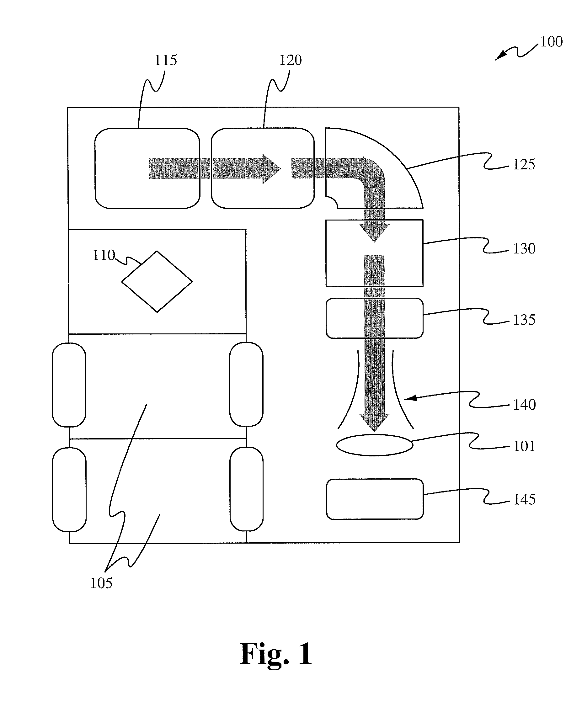
[0029]Systems in accordance with the invention are specifically tailored to fabricate specific semiconductor devices, such as solar cells. These systems use tolerances that are more relaxed than those required to fabricate other semiconductor devices. They fabricate devices more quickly, less expensively, and in a smaller space than do prior art systems. Such systems are capable of producing at least 1,000 solar cells per hour.

[0030]Systems are further simplified because no charge neutralization is used since wafers have no featured coverings, scanning is simplified, and mass analyses can be performed using other methods. All of these advantages result in an output higher than can be realized using traditional semiconductor fabrication systems.

[0031]Systems in accordance with the embodiments also produce more efficient solar cells, solar cells with doping profiles tailored to reduce ohmic losses and the effects of dead layers.

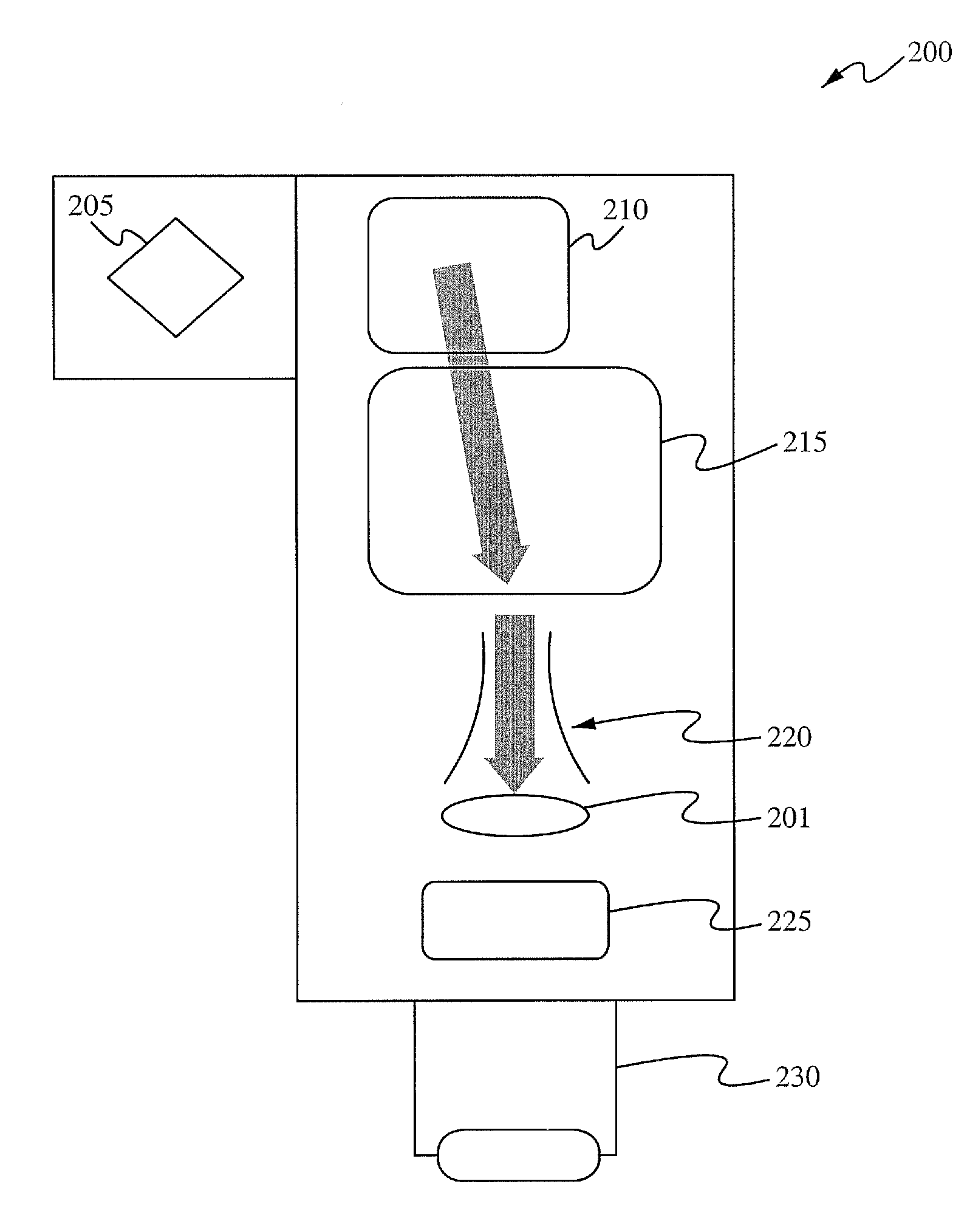
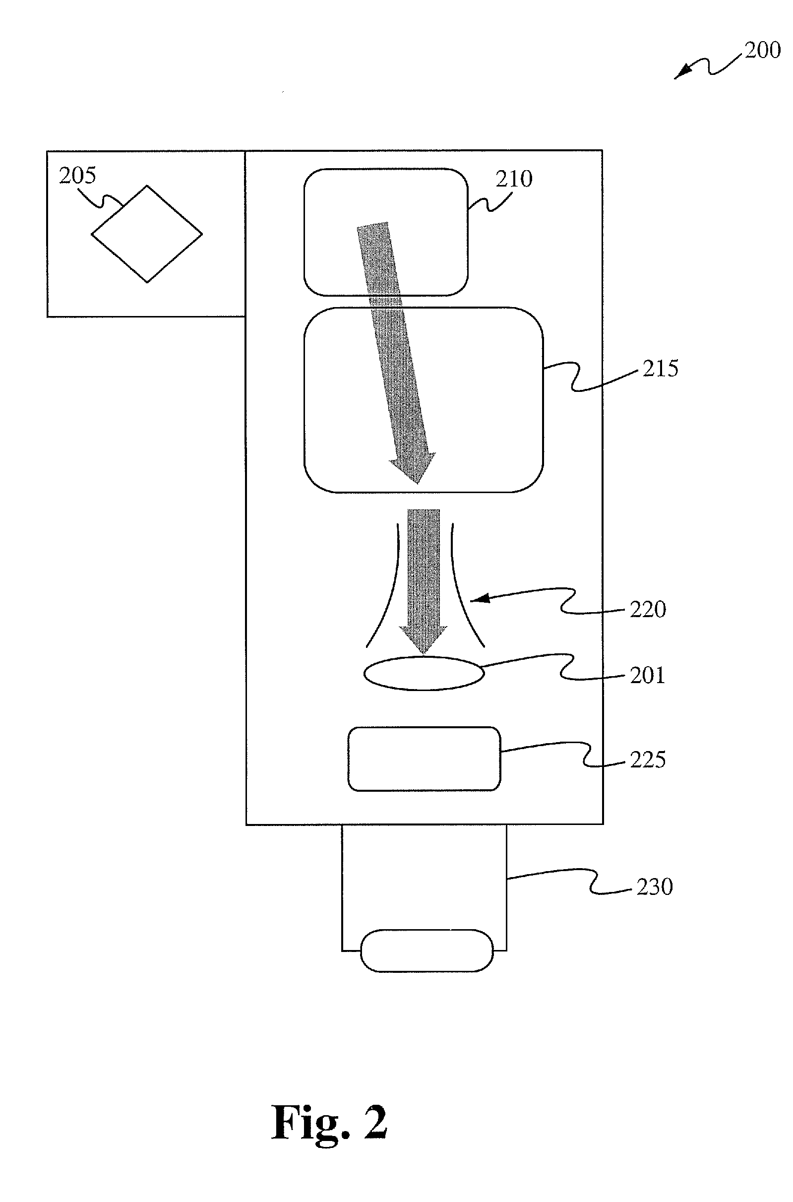
[0032]FIG. 2 shows a system 200 for fabricating solar cel...


PUM


Abstract

Solar cells and other semiconductor devices are fabricated more efficiently and for less cost using an implanted doping fabrication system. A system for implanting a semiconductor substrate includes an ion source (such as a single-species delivery module), an accelerator to generate from the ion source an ion beam having an energy of no more than 150 kV, and a beam director to expose the substrate to the beam. In one embodiment, the ion source is single-species delivery module that includes a single-gas delivery element and a single-ion source. Alternatively, the ion source is a plasma source used to generate a plasma beam. The system is used to fabricate solar cells having lightly doped photo-receptive regions and more highly doped grid lines. This structure reduces the formation of “dead layers” and improves the contact resistance, thereby increasing the efficiency of a solar cell.

Description

RELATED APPLICATION [0001]This application claims priority under 35 U.S.C. §119(e) to the co-pending U.S. Provisional Application Ser. No. 61 / 131,687, filed Jun. 11, 2008, entitled “SOLAR CELL FABRICATION USING IMPLANTATION,” co-pending U.S. Provisional Application Ser. No. 61 / 131,688, filed Jun. 11, 2008, entitled “APPLICATIONS SPECIFIC IMPLANT SYSTEM FOR USE IN SOLAR CELL FABRICATIONS,” co-pending U.S. Provisional Application Ser. No. 61 / 131,698, filed Jun. 11, 2008, entitled “FORMATION OF SOLAR CELL- SELECTIVE EMITTER USING IMPLANTATION AND ANNEAL METHODS,” and co-pending U.S. Provisional Application Ser. No. 61 / 133,028, filed Jun. 24, 2008, entitled “SOLAR CELL FABRICATION WITH FACETING AND IMPLANTATION,” co-pending U.S. Provisional Application Ser. No. 61 / 210,545, filed Mar. 20, 2009, entitled “ADVANCED HIGH EFFICIENCY CRYSTALLINE SOLAR CELL FABRICATIONS METHOD,” which are all hereby incorporated by reference as if set forth herein.FIELD OF THE INVENTION [0002]This invention re...

Claims


Application Information

Patent Timeline
Patent Type & Authority Applications(United States)
IPC IPC(8): H01J3/14H01J37/08H01L31/18H01L21/265
CPCH01L21/26513H01L21/266Y02E10/547H01L31/072H01L31/1804H01L31/022425H01L21/2658Y02P70/50H01L31/04H01L31/18H01L21/265H01L31/0236H01L21/26506
Inventor ADIBI, BABAKMURRER, EDWARD S.
Owner INTEVAC
Why Eureka
Try Eureka