Solid-state imaging device, driving method thereof, and camera

a solid-state imaging and driving method technology, applied in the direction of solid-state device signal generators, picture signal generators, television systems, etc., can solve the problems of increasing the time required for counting clocks, increasing the chip area and power consumption, increasing the circuit size, etc., to prevent s/n deterioration, high practical value of the present invention, and optimizing the gains for each color

Inactive Publication Date: 2009-12-17
PANASONIC CORP
View PDF8 Cites 46 Cited by
  • Summary
  • Abstract
  • Description
  • Claims
  • Application Information

AI Technical Summary

Benefits of technology

[0019]According to the solid-state imaging device of the present invention, it is possible to optimize the gains for each color without the need for complicated control of changing the resistance values of variable resistances and switching the switches depending on the pixels from which signals are to be read, while preventing an S/N deterioration in the AD conversion.
[0020]Thus, the practical value of the present inventio

Problems solved by technology

However, the conventional approach of increasing the number of bits of the AD converters for the purpose of white balance entails a problem that a time required for counting clocks increases in the case where AD conversion is performed by using a ramp waveform for the reference signal and by counting clocks from when the reference signal starts to be varied until a comparator of the corresponding column shows a match between a pixel signal and the reference signal, as disclosed in Patent Reference 2.
In addition, although one may propose parallel processing using a plurality of comparator circuits as above and the like to increase the number of bits, such a structure results in an increase in the circuit size, causing a problem of a

Method used


Image

  • Solid-state imaging device, driving method thereof, and camera
  • Solid-state imaging device, driving method thereof, and camera
  • Solid-state imaging device, driving method thereof, and camera

Examples


embodiment 1

[0041]First, Embodiment 1 of the present invention shall be described.

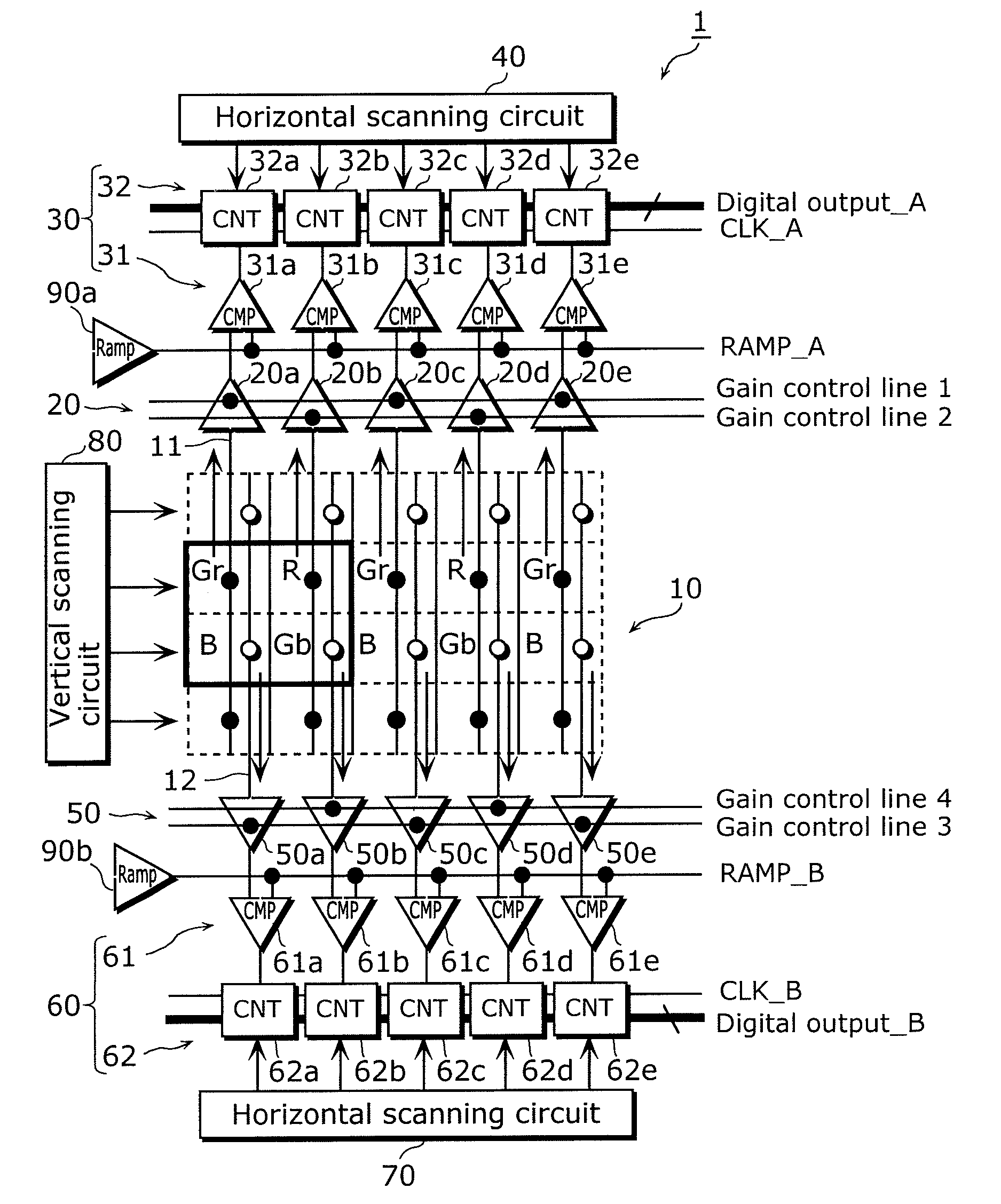
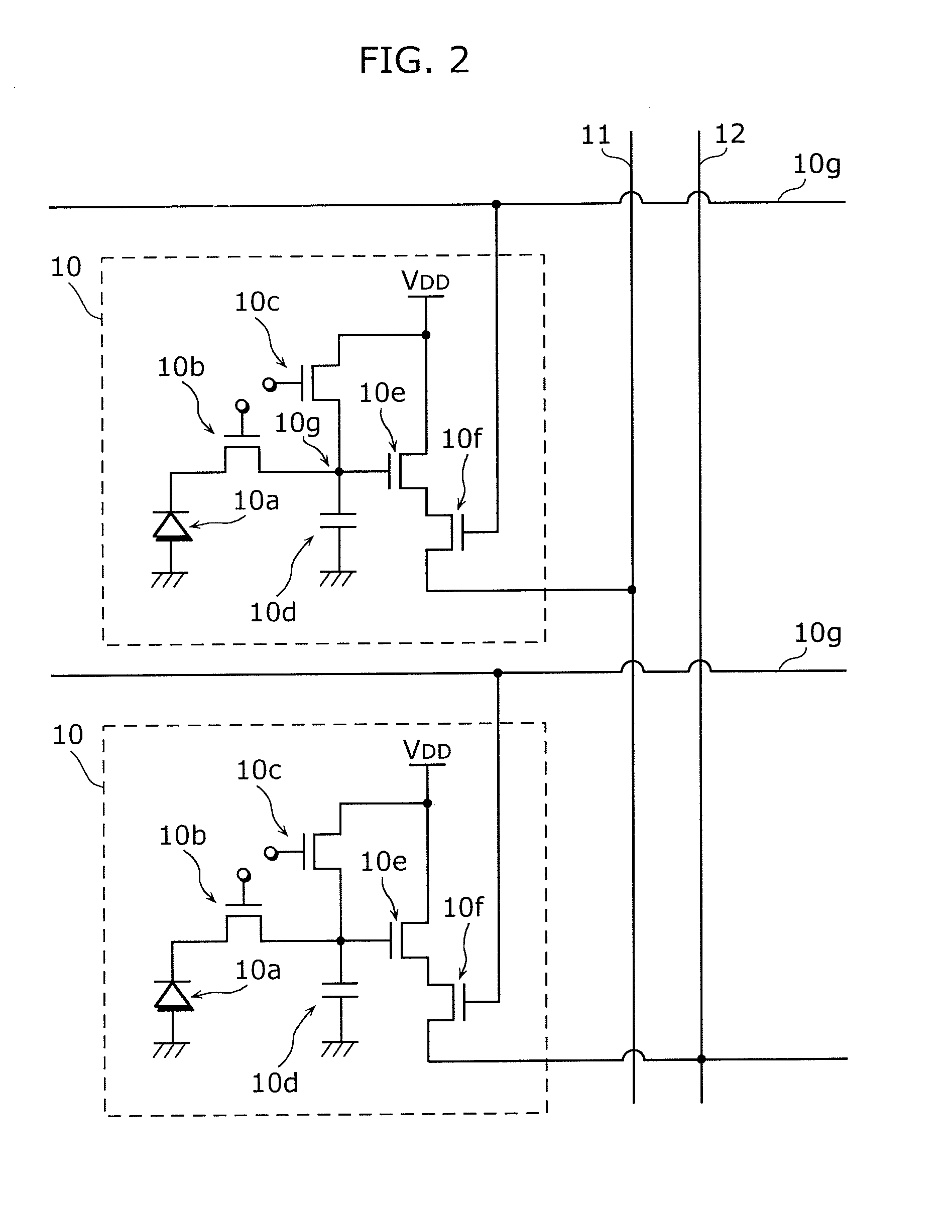
[0042]FIG. 1 is a circuit block diagram of a solid-state imaging device 1 according to Embodiment 1 of the present invention. The solid-state imaging device 1 is a color image sensor including pixels 10 that are formed on a semiconductor substrate and convert light into electric signals. It is characterized in including: column amplifiers 20 (20a to 20e) and 50 (50a to 50e) each provided independently for a corresponding color among, for example, RGB (Red, Blue, and Green); and column AD converters 30 (31a to 31e and 32a to 32e) and 60 (61a to 61e and 62a to 62e) each provided independently for a corresponding color. The column AD converters 30 and 60 include: comparators 31 (31a to 31e) and 61 (61a to 61e) that compare signals; and counters 32 (32a to 32e) and 62 (62a to 62e) that count the clocks until a time point determined by a comparison by the comparators 31 and 61 between a pixel signal and a ramp signal. ...

embodiment 2

[0079]Next, Embodiment 2 of the present invention shall be described.

[0080]FIG. 10 is a circuit block diagram of a solid-state imaging device 2 according to Embodiment 2 of the present invention. The solid-state imaging device 2 is characterized in setting column AD converter gains which differ depending on the colors of RGB. It includes a plurality of pixels 10, a plurality of column amplifiers 20 and 50, a plurality of column AD converters 30 and 60, horizontal scanning circuits 40 and 70, a vertical scanning circuit 80, and ramp signal generating units 91 to 94.

[0081]The solid-state imaging device 2 is different from that of Embodiment 1 in that it includes four ramp signal generating unit 91 to 94 instead of two ramp signal generating units 90a and 90b in Embodiment 1. Other aspects are the same as Embodiment 1. Hereinafter, the same structural elements as those of Embodiment 1 are denoted with the same reference numerals, and the descriptions thereof shall be omitted.

[0082]The ...


PUM


Abstract

A solid-state imaging device which optimizes gains for each color without a need for complicated control of changing the resistance values of variable resistances and switching switches depending on pixels from which signals are to be read, while preventing an S/N deterioration in AD conversion. The solid-state imaging device comprises: a plurality of pixels arranged in a matrix; column amplifiers, each amplifying signals generated by pixels of a corresponding one of columns of the matrix; and column AD converters, each performing AD conversion on a signal generated by a corresponding one of the column amplifiers, wherein each of the plurality of pixels corresponds to a color among colors, and each of the column amplifiers amplifies output signals generated by all pixels of a corresponding one of the colors, among pixels of the corresponding column of the matrix.

Description

BACKGROUND OF THE INVENTION[0001](1) Field of the Invention[0002]The present invention relates to a solid-state imaging device that converts light into electric signals, and relates particularly to a solid-state imaging device provided with an amplifier and an AD converter for each column of pixels arranged in a matrix.[0003](2) Description of the Related Art[0004]Color solid-state imaging devices (color image sensors) require white balance to adapt to changes in the color temperature and so on of the object. For example, the colors of the object vary depending on types of light (sunlight and fluorescent light, for example), and thus, to suit the color temperature in each scene, solid-state imaging devices need processing that makes white color of the object appear white even in image signals.[0005]Conventionally, the following has been performed for the purpose of white balance: the number of bits (resolution) of the AD converters is increased so that 1 to 2 bits are used for a dig...

Claims


Application Information

Patent Timeline
IPC IPC(8): H04N5/00H04N9/04
CPCH04N5/378H04N9/735H04N9/045H04N25/70H04N25/75H04N25/134H04N23/88
Inventor MASUYAMA, MASAYUKIKYOGOKU, MASANORI
Owner PANASONIC CORP
Why Eureka
Try Eureka