Wide aperture image sensor pixel

Active Publication Date: 2009-12-17
OMNIVISION TECH INC
View PDF10 Cites 13 Cited by
  • Summary
  • Abstract
  • Description
  • Claims
  • Application Information

AI Technical Summary

Benefits of technology

[0009]The present invention has the advantage of increasing the area of the

Problems solved by technology

The primary disadvantages are reduced sensitivity because the pixel area is smaller, and the smaller open

Method used


Image

  • Wide aperture image sensor pixel
  • Wide aperture image sensor pixel
  • Wide aperture image sensor pixel

Examples


Embodiment Construction

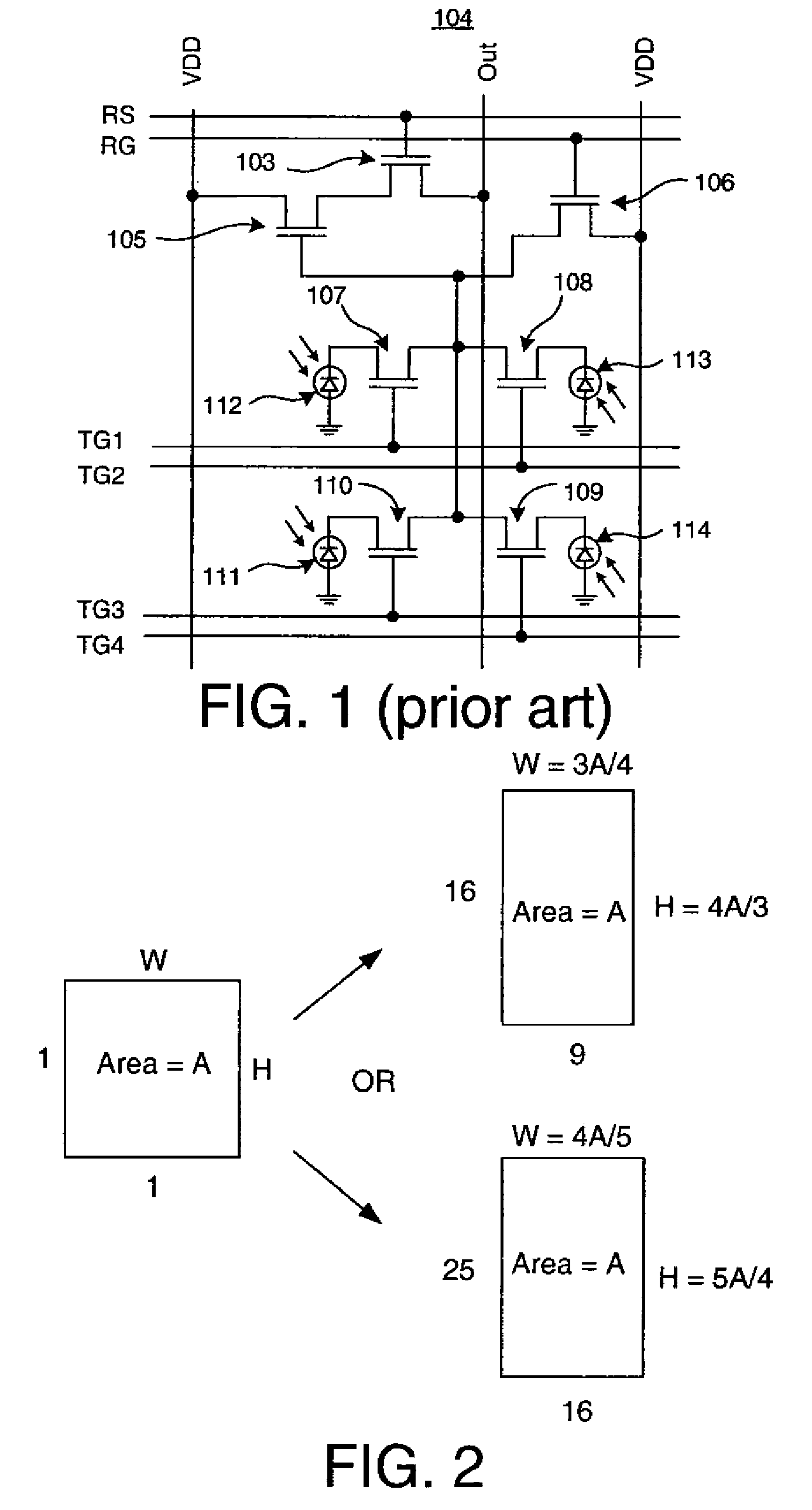
[0025]The present invention will first disclose the structure of a pixel with increased area of the opening between wires covering the photodiode. Referring to FIG. 2, the typical pixel has equal width, W, and height, H. So a 1.4 μm pixel is 1.4 μm square. There is no fundamental requirement that pixels must be square. The pixel aspect ratio can be changed so it has a height greater than width. This aspect ratio spaces out the horizontal wires. It reduces the space between vertical wires, but there are fewer vertical wires than horizontal wires. Therefore, there is a net increase in the opening for light between metal wires with a rectangular shaped pixel.

[0026]With rectangular pixels in the image sensor, the camera will use image processing to transform the rectangular pixels of the image sensor into one with square pixels for display. It is desirable to make the aspect ratio of the pixel be the ratio of two perfect squares such as 16:9 or 25:16 and other similar aspect ratios. Ref...


PUM


Abstract

An image sensor includes a unit cell of four pixels. The unit cell includes four photosensitive regions that collect charge in response to light; four transfer transistors that respectively pass the charge from each of the four photosensitive regions to one common charge-to-voltage conversion mechanism; three control wires in which a first control wire controls two of the transfer transistors and a second control wire controls one of the transfer transistors and a third control wire controls one of the transfer transistors; an amplifier connected to the common charge-to-voltage conversion mechanism that outputs an output signal in response to a signal from the charge-to-voltage conversion mechanism; and a reset transistor connected to the common charge-to-voltage conversion mechanism for resetting the charge-to-voltage conversion mechanism to a predetermined signal level.

Description

FIELD OF THE INVENTION[0001]The present invention generally relates to image sensors and more particularly to such image sensors having improved openings between the metal wires covering the photodiode for increasing sensitivity.BACKGROUND OF THE INVENTION[0002]As pixel sizes are reduced to less than 1.7 μm to meet demand, there are tradeoffs. The primary disadvantages are reduced sensitivity because the pixel area is smaller, and the smaller opening between pixel wires blocks too much light.[0003]For example, referring to FIG. 1, the pixel schematic from U.S. Patent Publication 2008 / 0062290 A1 is shown. The unit cell has four transfer gates 107, 108, 109, and 110 that control the flow of charge between the floating diffusion and photodiodes 112, 113, 114, and 111, respectively. Transistor 106 resets the floating diffusion to the level of the power supply VDD. Transistor 105 buffers the floating diffusion voltage and the row select transistor 103 switches that voltage onto the outpu...

Claims


Application Information

Patent Timeline
IPC IPC(8): H04N5/335
CPCH01L27/14603H01L27/14609H01L27/14636H01L27/14641H01L27/14689H04N5/347H04N5/37457H01L27/14645H04N25/46H04N25/778H01L27/146
Inventor PARKS, CHRISTOPHER
Owner OMNIVISION TECH INC
Why Eureka
Try Eureka