
Photoelectric semiconductor device capable of generating uniform compound lights

a photoelectric semiconductor and light-emitting diode technology, applied in the direction of semiconductor devices, basic electric elements, electrical equipment, etc., can solve the problems of only being able to use flip-chip type leds, increase manufacturing costs, and complicate the procedur

Inactive Publication Date: 2009-12-24
LITE ON TECH CORP +1
View PDF3 Cites 51 Cited by
  • Summary
  • Abstract
  • Description
  • Claims
  • Application Information

AI Technical Summary

Problems solved by technology

The extremely thin thickness of the phosphor layer 2 on the chip 1 greatly complicates the procedure and increases manufacture cost.
Such process can only be utilized for flip-chip type LED.
After improving the evenness of lights, the prior art can not further increase, or even maintain the light emission efficiency of the LED at the same time.

Method used


Image

  • Photoelectric semiconductor device capable of generating uniform compound lights
  • Photoelectric semiconductor device capable of generating uniform compound lights
  • Photoelectric semiconductor device capable of generating uniform compound lights

Examples


first embodiment

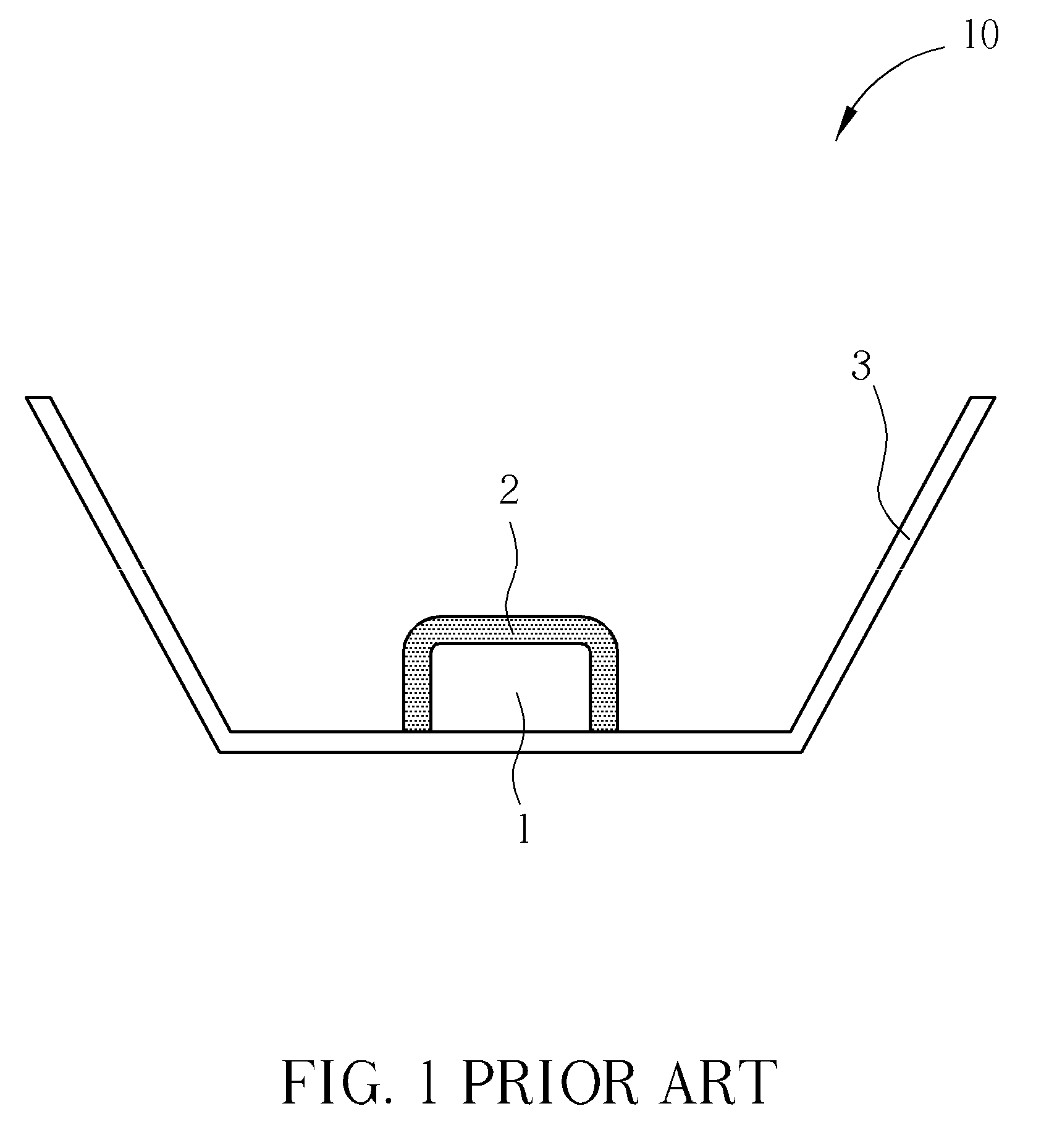
[0023]Please refer to FIG. 2. FIG. 2 is an illustration of a first exemplary embodiment of a light emitting diode (LED) 20 capable of generating uniform compound lights according to the present invention. The LED 20 includes a chip 21, a base 24, a first layer 23, and a second layer 22. The chip 21 is fixed on the base 24 and can be chips of direct-emitting, lateral-emitting, or flip-chip forms that can emit 400 nm 470 nm blue lights or 300 nm 400 nm ultraviolet lights. The base 24 can be a metal substrate, a printed circuit board (PCB), a ceramic substrate, a high polymer plastic substrate, a plastic leaded chip carrier (PCLL), or a substrate formed by other compound material. The inner first layer 23 covers directly on the chip 21 and in the embodiment, the first layer 23 can be transparent high polymer colloid such as epoxide, silica gel, or other high polymer compound and is used for separating the chip 21 and the second layer 22 to enhance the light emission efficiency. The tra...

second embodiment

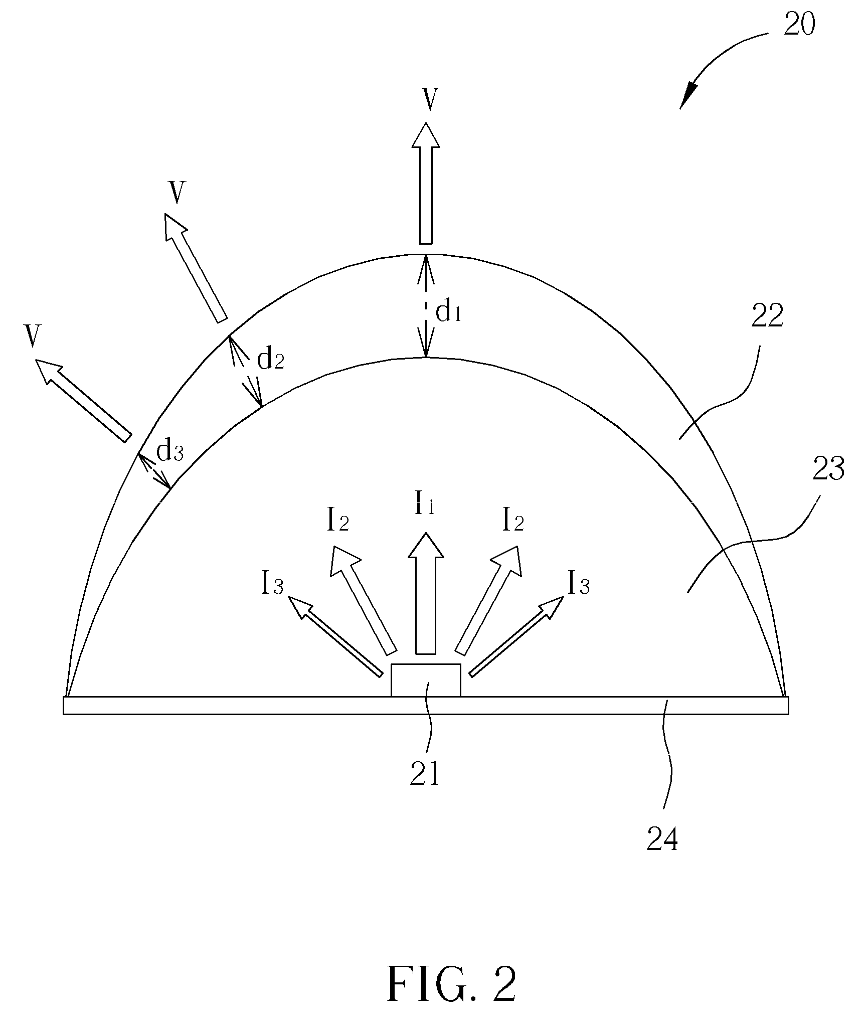
[0024]Please refer to FIG. 3. FIG. 3 is an illustration of a second exemplary embodiment of a light emitting diode (LED) 30 capable of generating uniform compound lights according to the present invention. The LED 30 includes a chip 31, a base 34, a first layer 33, and a second layer 32, where the chip 31 is fixed on the base 34. The second layer 32 is designed to have different concentration of phosphor powder in different section corresponding to different light emitting angle to generate uniform compound lights after the light passing through the second layer 32. For example, a first section of the second layer 32 has concentration D1 that corresponds to the light emitting strength I1, a second section has concentration D2 that corresponds to the light emitting strength I2, and a third section has concentration D3 that corresponds to the light emitting strength 13. In the second embodiment, D1>D2>D3, and the concentration of each section is further designed to satisfy the followi...


PUM


Abstract

A transparent layer and a phosphor layer are covered on the LED chip for increasing light emission efficiency and evenness of the LED. Based on angle-dependent emission strength of the LED chip, the phosphor layer is designed with different thickness or contains different phosphor powder concentration in different section. The lights emitted with different strength from different angle of the LED chip are transformed into uniform compound lights after passing through the phosphor layer that has different thickness or phosphor powder concentration. Micro structures capable of destroying the full reflection occurred on the incident lights are further configured on both the inner and outer surfaces of the phosphor layer to increase the light emission efficiency.

Description

BACKGROUND OF THE INVENTION[0001]1. Field of the Invention[0002]The present invention relates to a light emitting diode device, and more particularly, to a light emitting diode device with two layers and capable of generating uniform compound lights and having high light emission efficiency.[0003]2. Description of the Prior Art[0004]Light emitting diode (LED) has been outstanding in energy-saving lighting with its features of small size, long device lifetime, high durability, environmental friendliness, and low power consumption. Of all the LEDs, white light LED (or LED with compound lights) combines two or more monochromatic lights and has been widely used in indicating lamps and display devices in information technology, communications, and consumer electronics products. In addition to improving the light emission efficiency, the unevenness of lights from the LED also requires an urgent solution in the study of compound LED.[0005]Please refer to FIG. 1, which is an illustration of...

Claims


Application Information

Patent Timeline
IPC IPC(8): H01L33/00H01L33/50H01L33/54
CPCH01L33/507H01L2933/0091H01L33/54H01L33/508
Inventor WU, CHIA-HAOSU, HUNG-YUAN
Owner LITE ON TECH CORP
Features
  • Generate Ideas
  • Intellectual Property
  • Life Sciences
  • Materials
  • Tech Scout
  • Unparalleled Data Quality
  • Higher Quality Content
  • 60% Fewer Hallucinations
Learn More