Reference buffer circuits

a reference buffer and circuit technology, applied in the direction of electric variable regulation, process and machine control, instruments, etc., can solve the problems of increasing power consumption and noise of the reference buffer circuit b>1/b>, and it is difficult to design an internal closed-loop reference buffer circuit for high-resolution ad

Active Publication Date: 2009-12-24
MEDIATEK INC
View PDF7 Cites 12 Cited by
  • Summary
  • Abstract
  • Description
  • Claims
  • Application Information

AI Technical Summary

Problems solved by technology

However, the wide bandwidth causes the power consumption and noise of the reference buffer circuit 1 to be increased.
It is difficult to design an internal closed-loop reference buffer circuit for a high-resolution ADC.

Method used


Image

  • Reference buffer circuits
  • Reference buffer circuits
  • Reference buffer circuits

Examples


Embodiment Construction

[0027]The following description is of the best-contemplated mode of carrying out the invention. This description is made for the purpose of illustrating the general principles of the invention and should not be taken in a limiting sense. The scope of the invention is best determined by reference to the appended claims.

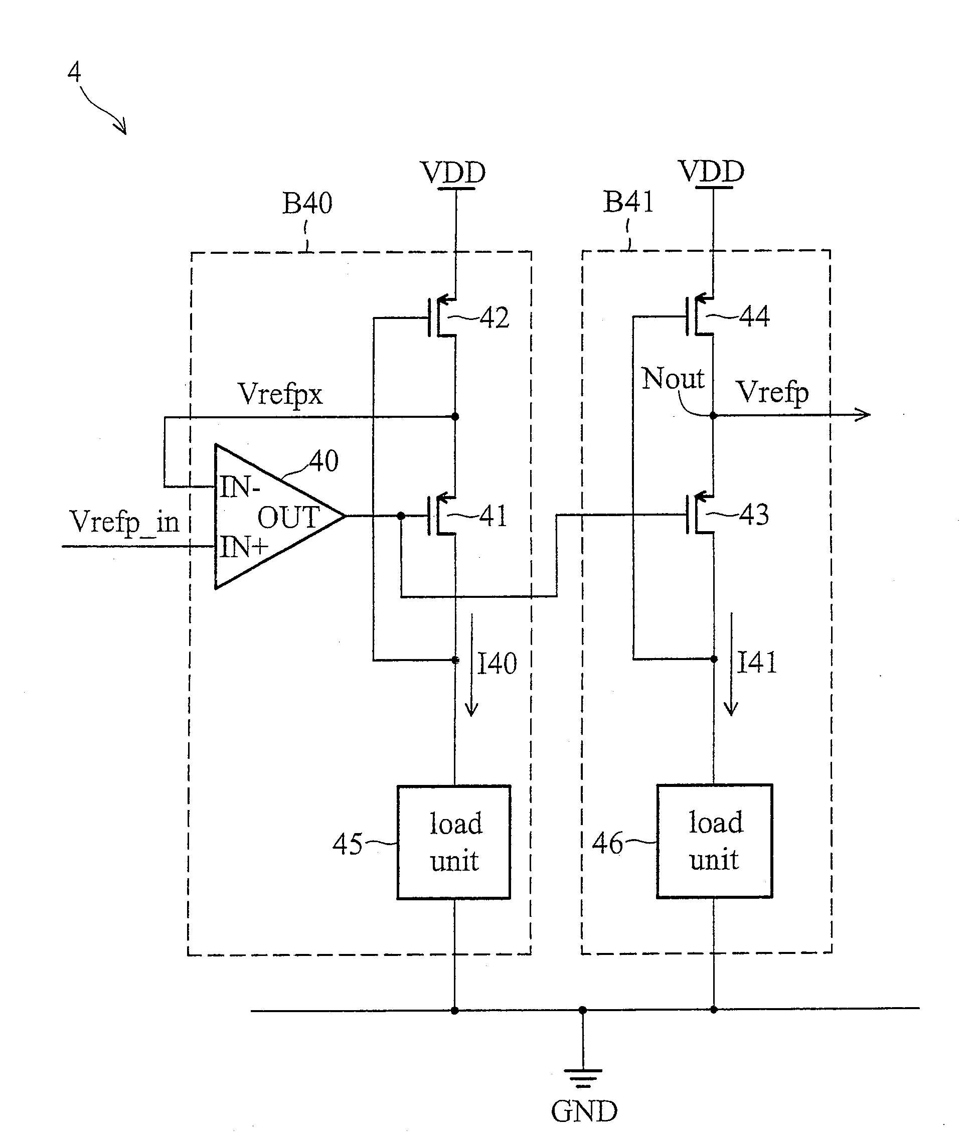
[0028]In an exemplary embodiment of a reference buffer circuit in FIG. 4, a single-ended reference buffer circuit 4 generates a reference voltage Vrefp at an output node Nout and comprises an amplifier 40, a P-type metal oxide semiconductor (PMOS) source-follower transistor 41, a PMOS driving transistor 43, PMOS current transistors 42 and 44, and load units 45 and 46. That is, in the single-ended reference buffer circuit 4, a closed-loop branch B40 comprises the amplifier 40, the PMOS transistors 41 and 42, and the load unit 45, and an open-loop branch B41 comprises the PMOS transistors 43 and 44 and the load unit 46.

[0029]In the closed-loop branch B40, a positive inpu...


PUM


Abstract

A reference buffer circuit provides a reference voltage at an output node and comprises a closed-loop branch comprising an amplifier and first and second MOS transistors and an open-loop branch comprising a third MOS transistor. A positive input terminal of the amplifier receives an input voltage. A gate of the first MOS transistor is coupled to the output terminal of the amplifier, and a source is coupled to a negative input terminal of the amplifier. A gate of the second MOS transistor is coupled to the drain of the first MOS transistor, a source is coupled to a first voltage source, and a drain is coupled to the source of the first MOS transistor. A gate of the third MOS transistor is coupled to the output terminal of the amplifier, and a source is coupled to the output node.

Description

BACKGROUND OF THE INVENTION[0001]1. Field of the Invention[0002]The invention relates to a reference buffer circuit, and more particularly to a reference buffer circuit for providing at least one reference voltage to an analog-to-digital converter, regulator or the like.[0003]2. Description of the Related Art[0004]Reference buffer circuits are required for high-speed and high-resolution analog-to-digital converters (ADCs). A reference buffer circuit usually comprises a reference buffer and provides at least one reference voltage to an ADC. There are two types of reference buffer circuits available for ADCs: closed-loop reference buffer circuits and open-loop reference buffer circuits.[0005]FIG. 1 shows a conventional closed-loop reference buffer circuit 1. An amplifier 10 has a negative feedback loop. The amplifier 10 receives an input voltage Vref_in at a positive input terminal and outputs a reference voltage Vref. The output impedance of the reference buffer circuit 1 is equal to...

Claims


Application Information

Patent Timeline
Patent Type & Authority Applications(United States)
IPC IPC(8): G05F3/08
CPCG05F1/56
Inventor LIAO, YING-MINLIN, YU-HSIN
Owner MEDIATEK INC
Why Eureka
Try Eureka