Method of forming a metal silicide layer, devices incorporating metal silicide layers and design structures for the devices

Inactive Publication Date: 2009-12-24
GLOBALFOUNDRIES INC
View PDF8 Cites 6 Cited by
  • Summary
  • Abstract
  • Description
  • Claims
  • Application Information

AI Technical Summary

Problems solved by technology

However, formation of devices using silicide layers in the wiring layers of in

Method used


Image

  • Method of forming a metal silicide layer, devices incorporating metal silicide layers and design structures for the devices
  • Method of forming a metal silicide layer, devices incorporating metal silicide layers and design structures for the devices
  • Method of forming a metal silicide layer, devices incorporating metal silicide layers and design structures for the devices

Examples


first embodiment

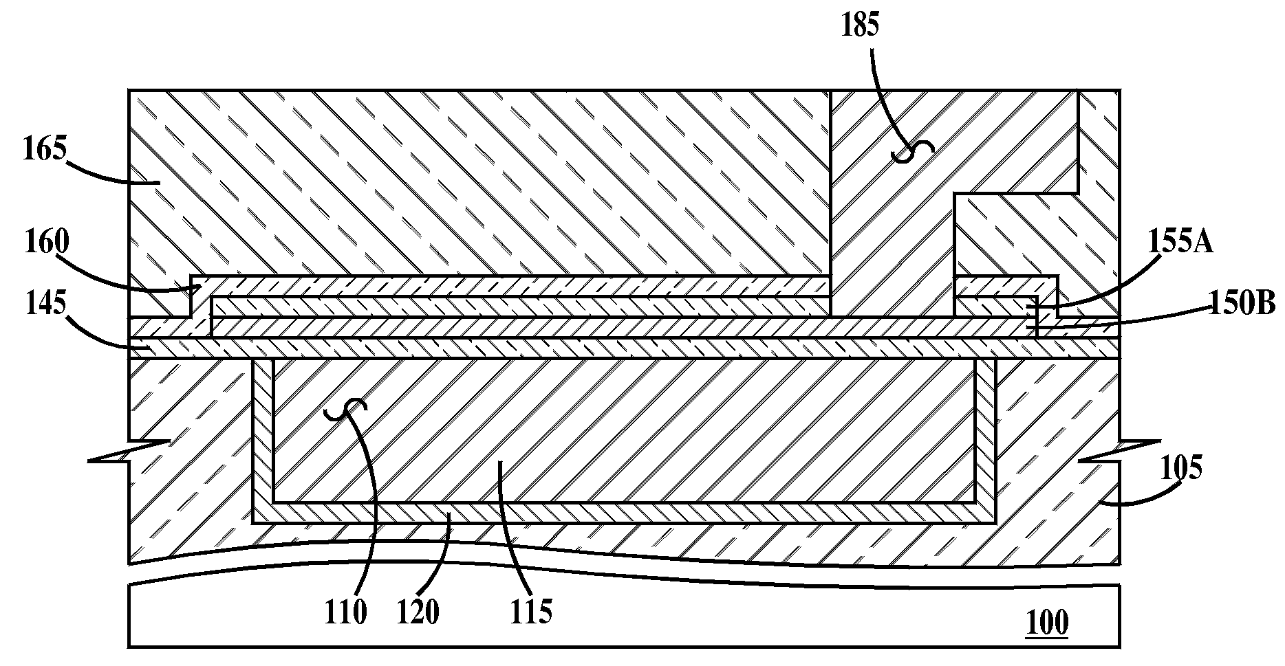
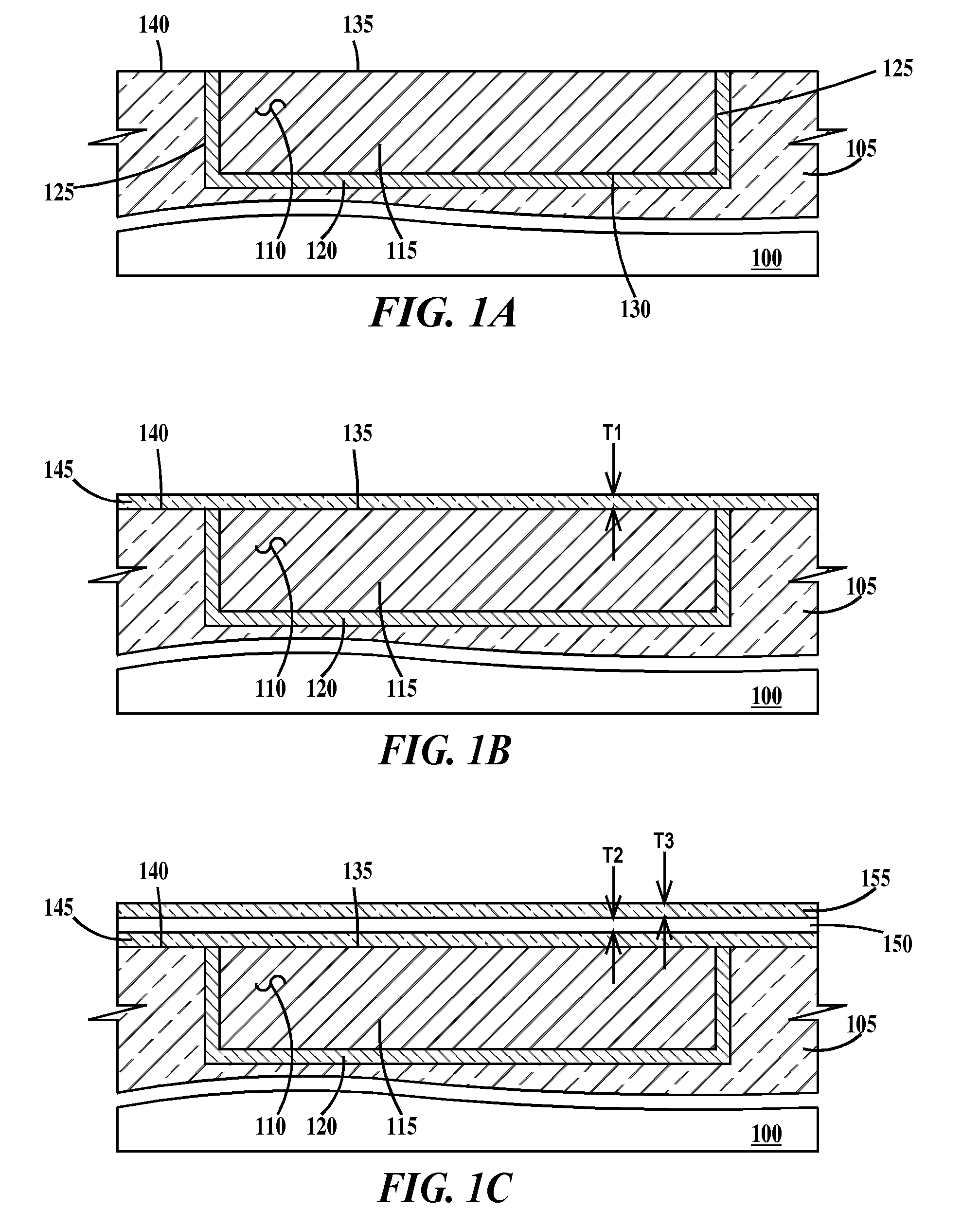
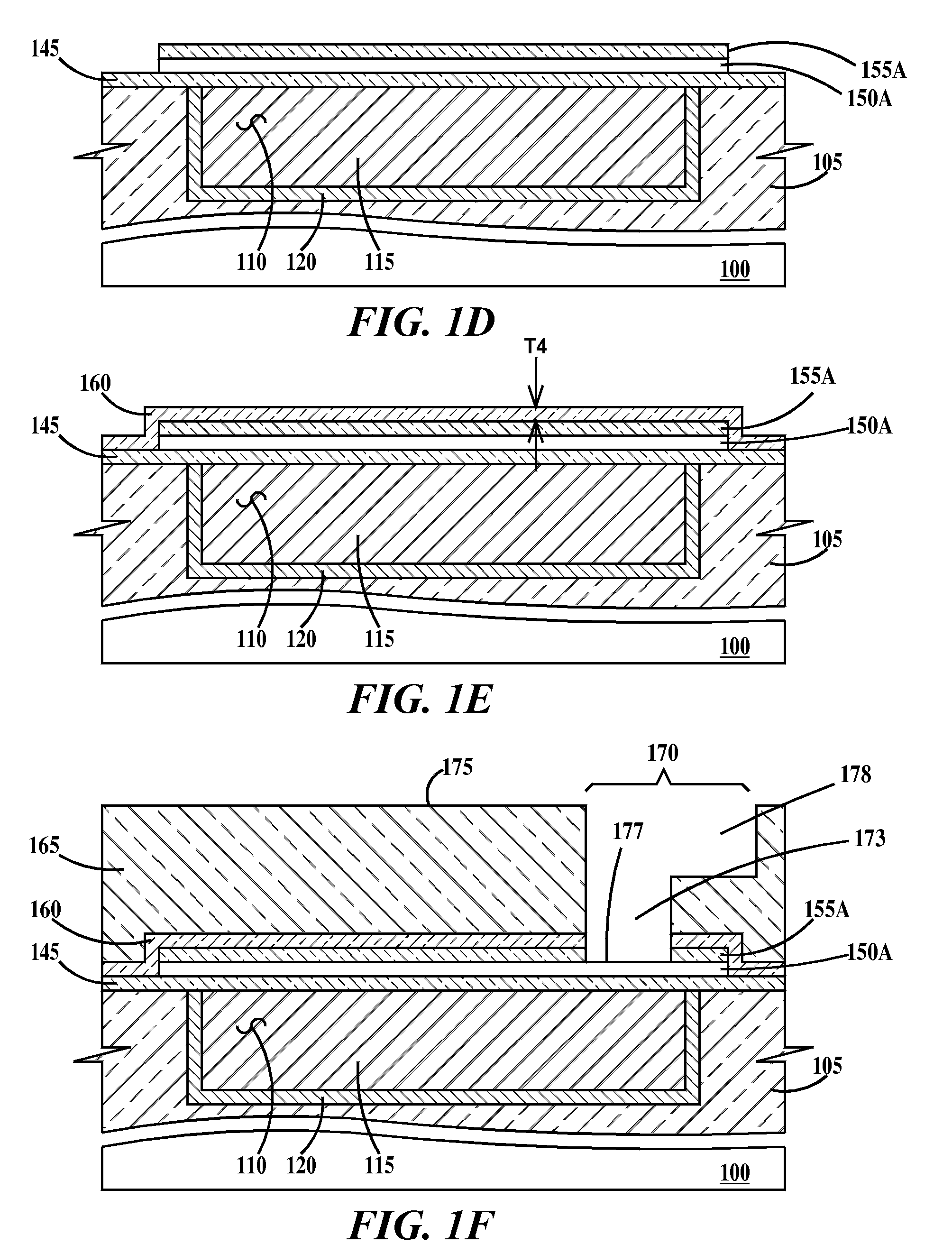
[0012]FIGS. 1A through 1I are cross-sectional drawings illustrating formation of a silicide layer and a capacitor according to present invention. In FIG. 1A, formed on a substrate 100 is a dielectric layer 105. Formed in dielectric layer 105 is a wire 110. Wire 110 comprises a core conductor 115 and an optional electrically conductive liner 120 formed on sidewalls 125 and a bottom surface 130 of wire 110. A top surface 135 of wire 110 is substantially coplanar with a top surface 140 of dielectric layer 105. In the example of FIG. 1A, wire 110 is a damascene formed by a damascene process (or dual damascene formed by a dual damascene process) wire.

[0013]A damascene process is one in which wire trenches or via openings are formed in a dielectric layer, an electrical conductor of sufficient thickness to fill the trenches is deposited on a top surface of the dielectric, and a chemical-mechanical-polish (CMP) process is performed to remove excess conductor and make the surface of the cond...

second embodiment

[0027]FIGS. 3A through 3I are cross-sectional drawings illustrating formation of a silicide layer and a capacitor according to present invention. FIG. 3A is similar to FIG. 1A except an additional wire 110A is formed in dielectric layer 105. Wire 110A is similar to wire 110 and comprises a core conductor 115A and an optional electrically conductive liner 120A. Wire 110A comprises the same materials as describes supra for wire 110. Wires 110 and 110A are advantageously formed simultaneously and comprise the same materials. A top surface 135A of wire 110A is substantially coplanar with top surface 140 of dielectric layer 105. In the example of FIG. 3A, wire 110A is a damascene formed by a damascene process (or dual damascene formed by a dual damascene process) wire.

[0028]In FIG. 3B, a first capping layer 145A is formed on top surface 135 of wire 110, top surface 135A of wire 110A and top surface 140 of dielectric layer 105. First capping layer 145A has a thickness T5. In one example, ...


PUM


Abstract

Methods of forming metal silicide layers. The methods include: forming a silicon-rich layer between dielectric layers; contacting the silicon-rich layer with a metal layer and heating the silicon rich-layer and the metal layer to diffuse metal atoms from the metal layer into the silicon layer to form a metal silicide layer.

Description

RELATED APPLICATIONS[0001]This application is related to copending United States Patent Application Docket Number BUR920080108US2.FIELD OF THE INVENTION[0002]The present invention relates to the field of integrated circuits; more specifically, it relates a method of forming a metal silicide layer, devices incorporating metal silicide layers and design structures incorporating a metal silicide layers.BACKGROUND OF THE INVENTION[0003]Integrated circuits utilize devices incorporating metal silicides. For example metal silicides are often used to form contact structures to the source, drain and gate electrode of field effect transistors. However, formation of devices using silicide layers in the wiring layers of integrated circuits has not been practiced, though such devices would be useful. Accordingly, there exists a need in the art to eliminate the deficiencies described hereinabove.SUMMARY OF THE INVENTION[0004]A first aspect of the present invention is a method, comprising: (a) for...

Claims


Application Information

Patent Timeline
IPC IPC(8): H01L21/768
CPCH01L21/76807H01L21/76886H01L23/5223H01L23/5228H01L23/53271H01L2924/0002H01L28/24H01L28/75H01L2924/00
Inventor ANDERSON, FELIX PATRICKHE, ZHONG-XIANGMCDEVIN, THOMAS LEDDYWHITE, ERIC JEFFREY
Owner GLOBALFOUNDRIES INC
Why Eureka
Try Eureka