Wireless IC device and manufacturing method thereof

a technology of ic device and manufacturing method, which is applied in the direction of printed circuit manufacturing, printed circuit aspects, instruments, etc., can solve the problems of increasing manufacturing cost, difficult to provide wiring on the inner circumferential surface of the recess formed by counterboring, and difficult to provide wiring having the shortest possible length, so as to reduce cost and prevent degradation of electrical properties

Inactive Publication Date: 2009-12-31
MURATA MFG CO LTD
View PDF4 Cites 86 Cited by
  • Summary
  • Abstract
  • Description
  • Claims
  • Application Information

AI Technical Summary

Benefits of technology

[0009]To overcome the problems described above, preferred embodiments of the present invention provide a wireless IC device w...

Problems solved by technology

Thus, the manufacturing cost is increased.
In addition, since a first main surface of the resin substrate having the recess and a semiconductor chip are connected, it is difficult to provide wiring on the inner circumferential surface of the recess formed by counterboring.
This makes it difficult to...

Method used


Image

  • Wireless IC device and manufacturing method thereof
  • Wireless IC device and manufacturing method thereof
  • Wireless IC device and manufacturing method thereof

Examples


first preferred embodiment

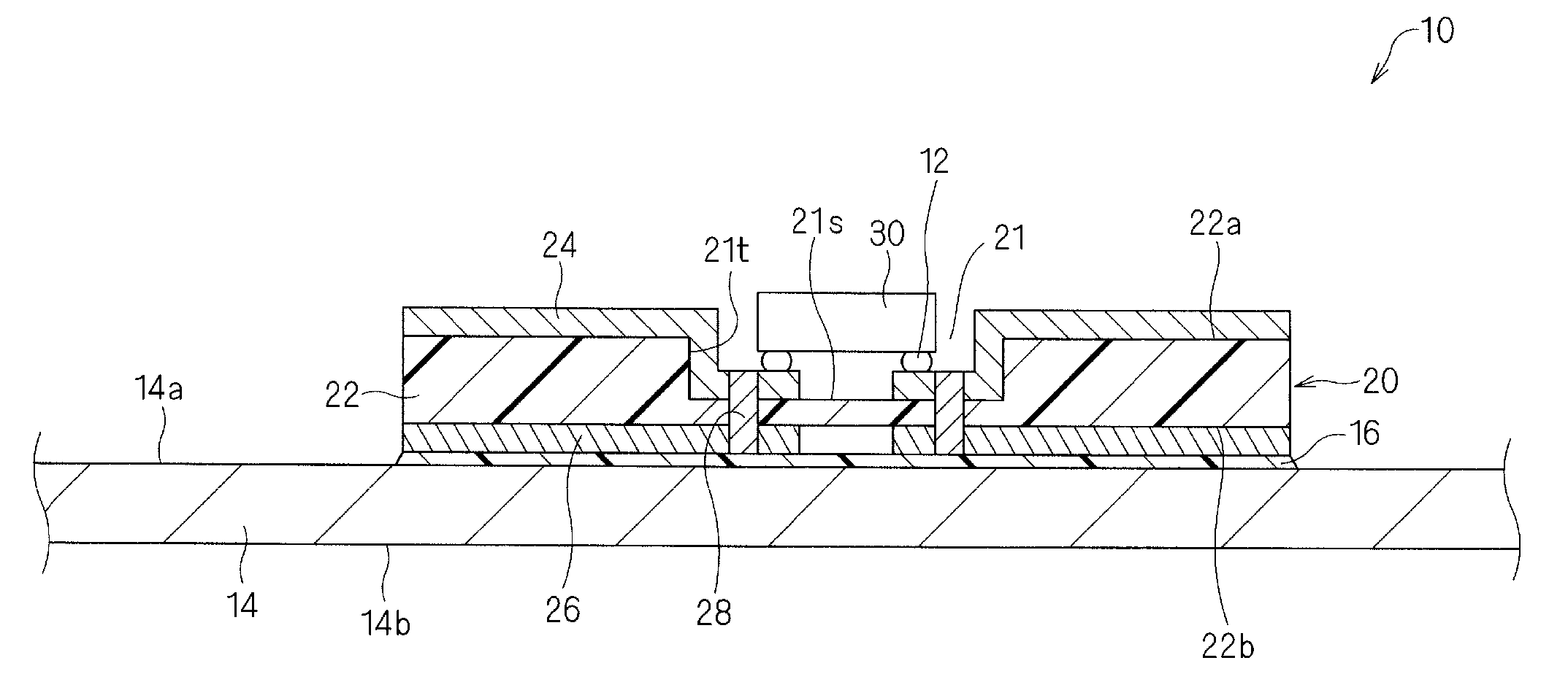
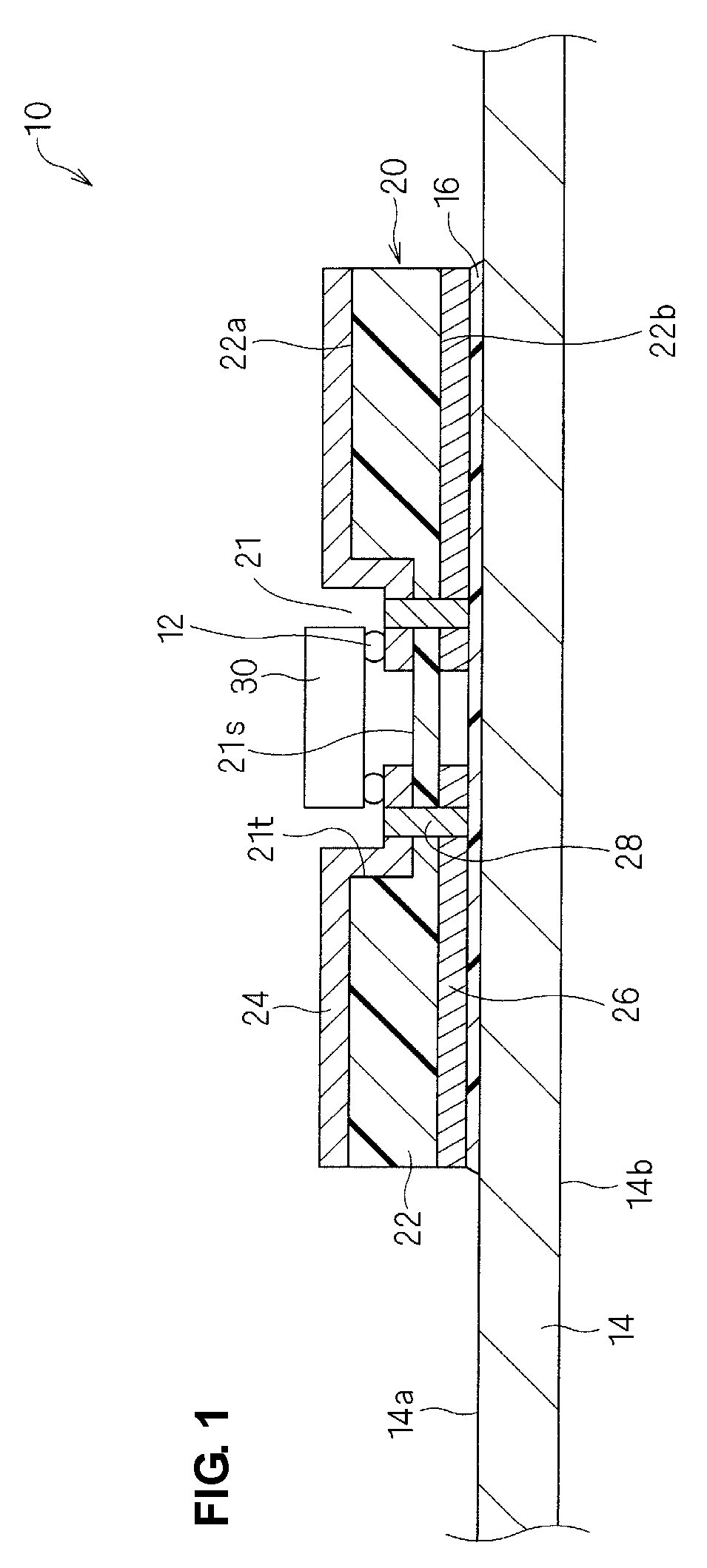
[0049]A wireless IC device 10 according to a first preferred embodiment of the present invention will be described with reference to FIGS. 1 to 4.

[0050]As shown in a sectional view in FIG. 1, the wireless IC device 10 is preferably formed by bonding a module 20, in which a wireless IC chip 30 is mounted in a recess 21 of a substrate 22, to a radiation plate 14 using a bonding material 16, such as an insulating adhesive sheet (an adhesive thin film on the adhesive surface of a commercially available seal) or an adhesive, for example. The radiation plate 14 includes a conductive material that is arranged in a predetermined shape.

[0051]The radiation plate 14 may preferably be formed, for example, by printing a resin including Ag particles on a sheet-shaped base and forming small wiring thereon by inkjet or photolithography and the base having the radiation plate 14 formed thereon may be bonded to a commodity, such as a package or container, for example.

[0052]While the radiation plate 1...

second preferred embodiment

[0075]A wireless IC device according to a second preferred embodiment of the present invention will be described with reference to FIGS. 5A to 5D and FIG. 6.

[0076]The wireless IC device according to the second preferred embodiment has a configuration substantially the same as that of the wireless IC device according to the first preferred embodiment. The difference between the second preferred embodiment and first preferred embodiment will be described and the same reference numerals will be assigned to the same or similar elements.

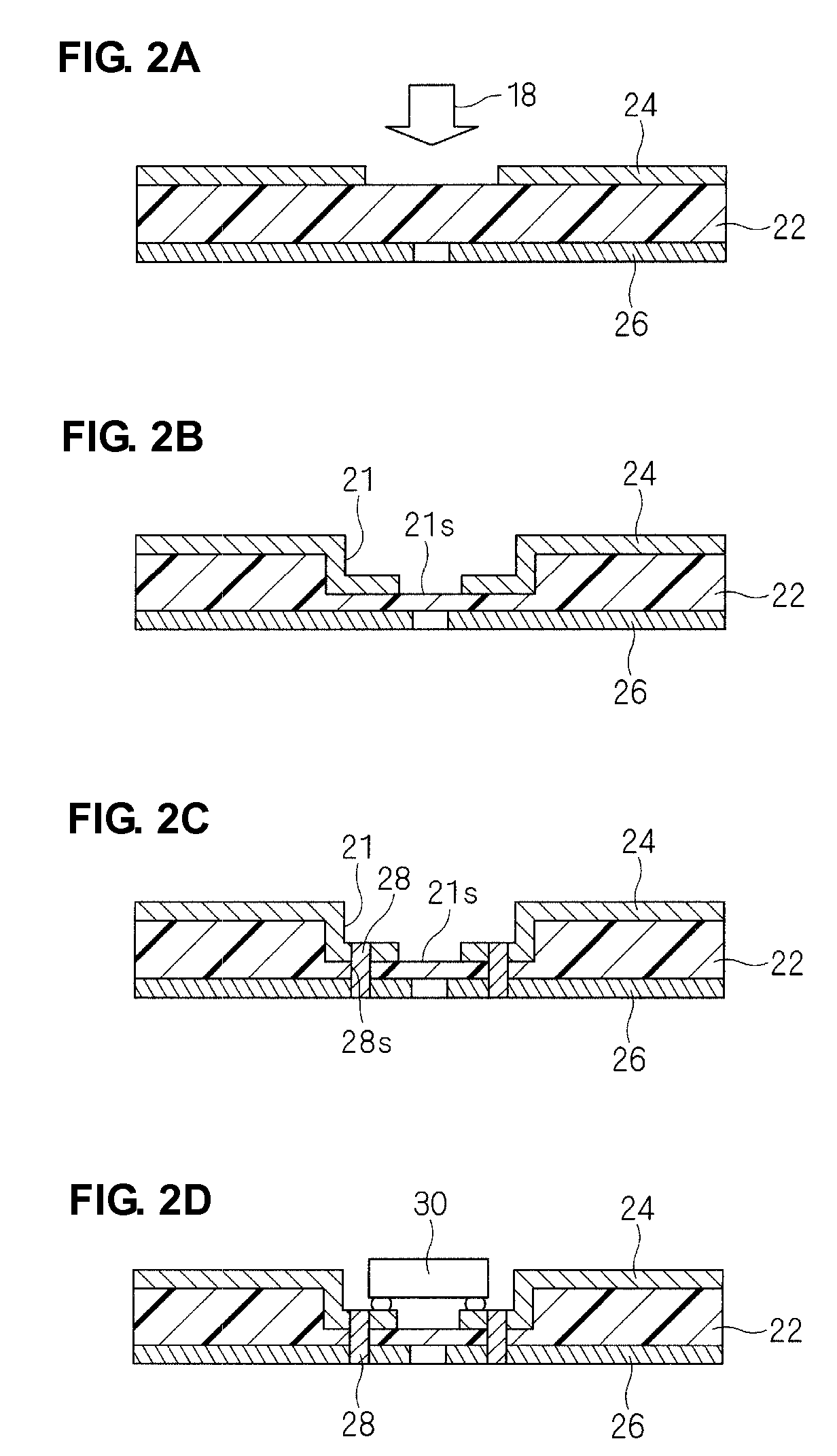
[0077]The wireless IC device according to the second preferred embodiment is different from the first preferred embodiment in the order of the steps for manufacturing the module. Hereafter, the steps for manufacturing the module will be described with reference to sectional views in FIGS. 5A to 5D and a main portion plan view in FIG. 6.

[0078]First, as shown in FIG. 5A, a metal foil-attached resin sheet is prepared and the metal foil is processed into a pr...

third preferred embodiment

[0092]A wireless IC device according to a third preferred embodiment of the present invention will be described with reference to FIGS. 7A to 7D and FIG. 8.

[0093]The wireless IC device according to the third preferred embodiment has a configuration substantially the same as that of the wireless IC device according to the first preferred embodiment. The wireless IC device according to the third preferred embodiment is different from the first preferred embodiment in the order of the steps for manufacturing the module 20. Hereafter, the steps for manufacturing the module 20 will be described with reference to a sectional views in FIGS. 7A to 7D and a main portion plan view shown in FIG. 8.

[0094]First, as shown in FIG. 7A, a metal foil-attached resin sheet is prepared and the metal foil is processed into a predetermined pattern by etching or other suitable method. Thus, the wiring patterns 24 and 26 are formed on both or one of the surfaces 22a and 22b of the resin sheet substrate 22. ...


PUM

PropertyMeasurementUnit
Sizeaaaaaaaaaa
Electrical conductoraaaaaaaaaa

Abstract

A wireless IC device includes a radiation plate, a wireless IC chip, and a substrate provided with a feed circuit that includes a resonant circuit and/or the matching circuit including an inductance element and that is electromagnetically coupled to the radiation plate. The substrate is made of a resin material. A recess is provided in a first main surface of the substrate. The substrate is provided with a wiring electrode arranged along a bottom surface and an inner circumferential surface of the recess and the first main surface of the substrate and electrically connected to the feed circuit, and a wedge member made of a different material from the resin material and extending between the bottom surface of the recess and a second main surface of the substrate spaced apart from the wiring electrode. The wireless IC chip is mounted in the recess and coupled to the wiring electrode.

Description

BACKGROUND OF THE INVENTION[0001]1. Field of the Invention[0002]The present invention relates to a wireless IC device and a manufacturing method thereof. More specifically, the present invention relates to a wireless IC device, such as a non-contact wireless IC medium or a non-contact wireless IC tag, for example, used in an RFID (radio frequency identification) system, and a manufacturing method thereof[0003]2. Description of the Related Art[0004]Wireless IC devices including a module in which a wireless IC chip is mounted on a substrate and a radiation plate have been developed. In such a wireless IC device, a recess is provided in the substrate and the wireless IC chip is mounted in the recess.[0005]Japanese Unexamined Patent Application Publication No. 2004-319848 discloses a semiconductor apparatus manufactured by forming a wiring substrate by bonding copper bumps 116a and 118a and wiring patterns 117 and 119 to both surfaces of a resin substrate 110 with prepregs 120 therebetw...

Claims


Application Information

Patent Timeline
IPC IPC(8): G06K7/00H05K3/00
CPCG06K19/07749Y10T29/49124H01L23/49822H01L23/49827H01L23/49855H01L24/16H01L24/97H01L2224/13139H01L2224/13144H01L2224/16H01L2924/01079H01L2924/14H01L2924/3011H05K1/112H05K1/183H05K3/0061H05K2201/10674H05K2203/0278H01L2924/07802H01L23/13H01L2924/00
Inventor KATO, NOBORUSASAKI, YUTAKAOZAWA, MASAHIRO
Owner MURATA MFG CO LTD
Why Eureka
Try Eureka