Solid-state imaging device and camera

Active Publication Date: 2009-12-31
PANASONIC CORP
View PDF19 Cites 55 Cited by
  • Summary
  • Abstract
  • Description
  • Claims
  • Application Information

AI Technical Summary

Benefits of technology

[0041]This reduces the cost of manufactu

Problems solved by technology

However, when subtracting the reference signal of IR pixels from the signal output of RGB pixels, the IR signals contained in the signal output obtained from the RGB pixels cannot

Method used


Image

  • Solid-state imaging device and camera
  • Solid-state imaging device and camera
  • Solid-state imaging device and camera

Examples


Example

Embodiment 1

[0068]First, the structure of a digital still camera according to the embodiments of the present invention shall be described.

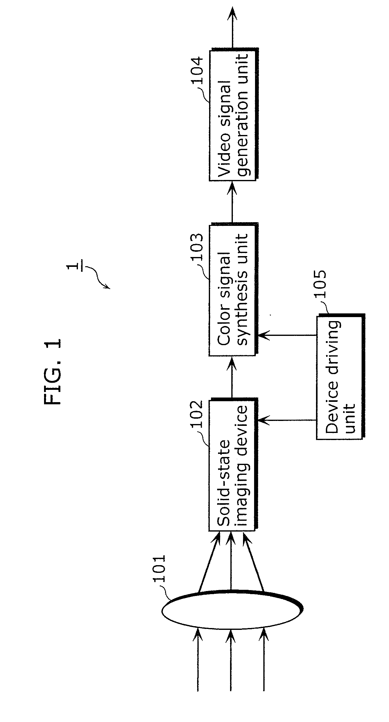
[0069]FIG. 1 is a block diagram illustrating a fundamental functional structure of a digital still camera according to Embodiment 1.

[0070]As shown in FIG. 1, a digital still camera 1 according to the present embodiment includes a lens 101, a solid-state imaging device 102, a color signal synthesis unit 103, a video signal generation unit 104, and a device driving unit 105.

[0071]From light incident on the digital still camera 1, the lens 101 forms an image on an imaging area of the solid state imaging device 102.

[0072]The solid-state imaging device 102 is a MOS image sensor or the like which generates color signals by photoelectrically converting the incident light.

[0073]The device driving unit 105 is a circuit which read out the color signals from the solid-state imaging device 102.

[0074]The color signal synthesis unit 103 is a DSP or the like whi...

Example

Embodiment 2

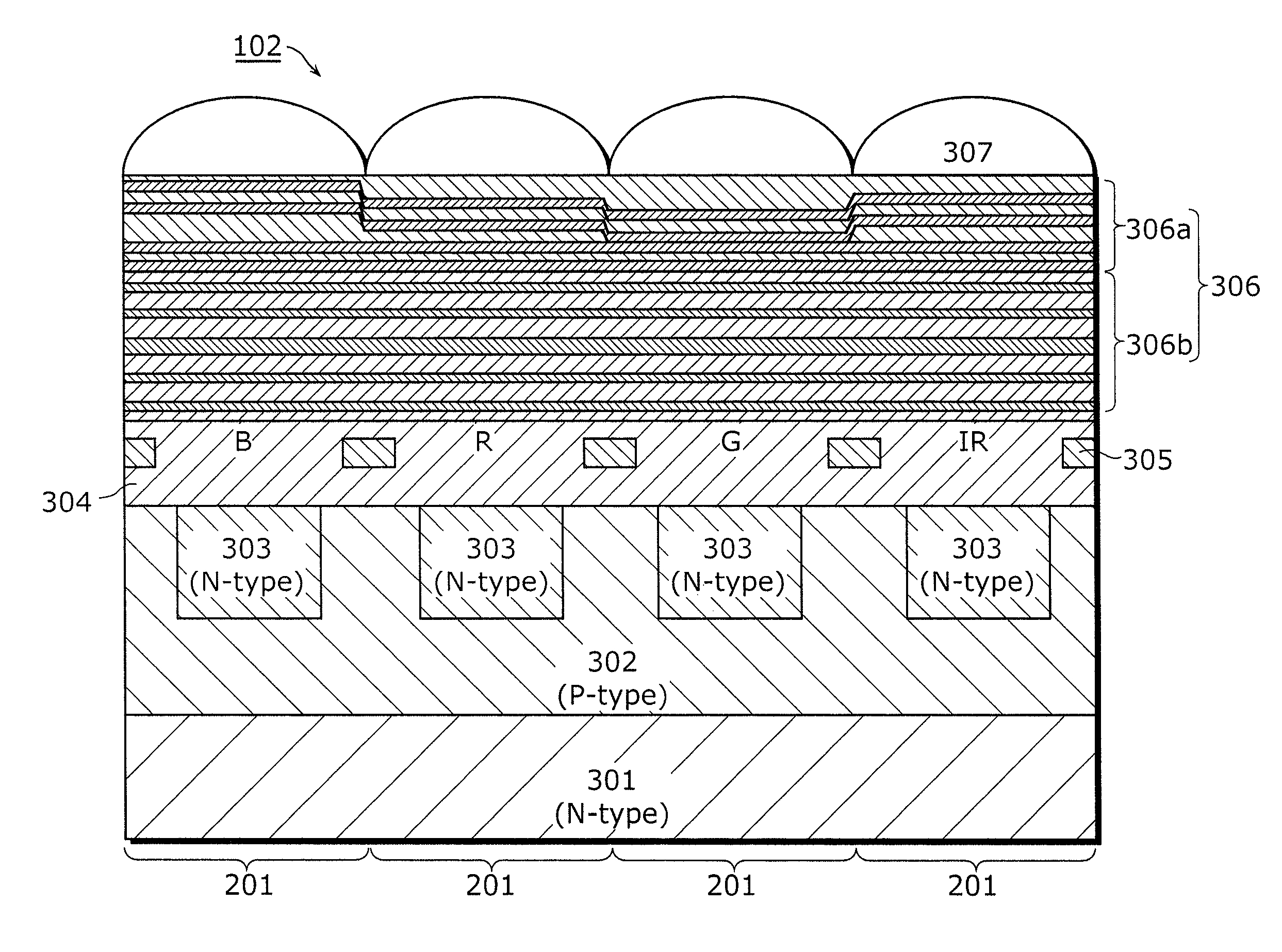
[0116]FIG. 5 is a cross-section diagram of unit pixels 201 of a solid-state imaging device 102 according to Embodiment 2. The solid-state imaging device 102 of Embodiment 2 is different from that of Embodiment 1 in film structure of the visible-light and near-infrared filter 306a. The near-infrared normalization filter 306b and the other structure are the same as that in Embodiment 1 and thus the descriptions thereof shall be omitted.

[0117]FIGS. 6A to 6E illustrate the structure and spectral characteristics of a color separation filter 306 of the solid-state imaging device 102 according to Embodiment 2.

[0118][Structure and Transmission Characteristics of Visible-Light and Near-Infrared Filter]

[0119]FIG. 6A illustrates a conceptual structure of a visible-light and near-infrared filter 306a, which allows color separation of visible light, of a color separation filter 306. The visible-light and near-infrared filter 306a has a layered structure described below.

[0120]When inc...

Example

Embodiment 3

[0137]FIGS. 7A to 7E illustrate the structure and spectral characteristics of a color separation filter 306 of a solid-state imaging device 102 according to Embodiment 3. The solid-state imaging device 102 in Embodiment 3 is different from that in Embodiment 2 in that a second spacer layer 433 is inserted in the R pixel (pixel in the red region) of the near-infrared normalization filter 306b. The other structure is the same as that in Embodiment 2 and thus the description thereof shall be omitted.

[0138][Structure and Transmission Characteristics of Near-Infrared Normalization Filter]

[0139]The near-infrared normalization filter 306b has a layered structure described below. When incident light has a set wavelength of λ2 (850 [nm], for example), the near-infrared normalization filter 306b has two λ / 4 multilayer films each of which is formed with layers that are having an optical thickness of approximately ¼ of the set wavelength of λ2 and are made of two types of materials ...


PUM


Abstract

A solid-state imaging device having a color filter with high color reproducibility even in the case of using lighting of low color temperatures. The solid-state imaging device has a plurality of pixels arranged two-dimensionally, and comprises a color separation filter which allows transmission of light of a predetermined wavelength in incident light for each of the plurality of pixels, wherein the color separation filter includes: a visible-light and near-infrared filter having transmission bands in regions of a visible lo wavelength band and a near-infrared wavelength band; and a near-infrared normalization filter laminated with the visible-light and near-infrared filter, wherein the near-infrared normalization filter is substantially transparent in the visible wavelength band and a first near-infrared wavelength band, and is substantially not transparent in a second near-infrared wavelength band between the visible wavelength band and the first near-infrared wavelength band.

Description

BACKGROUND OF THE INVENTION[0001](1) Field of the Invention[0002]The present invention relates to a solid-state imaging device and a camera, and in particular to a technique of color separation by using a color filter of a solid-state imaging device that detects visible light and near-infrared light.[0003](2) Description of the Related Art[0004]In recent years, the range of application for solid-state imaging devices such as digital cameras and mobile phones has been expanding rapidly, and colorization has become essential in any field.[0005]FIGS. 8A and 8B are diagrams related to a solid-state imaging device according a conventional art. FIG. 8A illustrates an array of pixels of the solid-state imaging device according the conventional art. FIG. 8B illustrates the spectral characteristics of the pixels of the solid-state imaging device according the conventional art.[0006]As shown in FIGS. 8A and 8B, an infrared cut filter is removed, and an infrared light filter (IR filter) that a...

Claims


Application Information

Patent Timeline
IPC IPC(8): H01L31/0232G02B5/20G02B5/28
CPCG02B5/201H01L27/14621G02B5/282
Inventor KASANO, MASAHIROKOYAMA, SHINZO
Owner PANASONIC CORP
Why Eureka
Try Eureka