Electrophoretic display device and electronic apparatus

a display device and display device technology, applied in the direction of static indicating devices, instruments, optics, etc., can solve the problems of increasing the consumption of current for driving a driver, reducing the time required for completing display, and visually recognizing jaggies (saw tooth shapes)

Active Publication Date: 2010-01-07
E INK CORPORATION
View PDF10 Cites 17 Cited by
  • Summary
  • Abstract
  • Description
  • Claims
  • Application Information

AI Technical Summary

Benefits of technology

[0022]An advantage of some aspects of the invention is that it provides an electrophoretic display device capable of representing a smooth contour in display and suppressing generation of undesirable leakage currents.

Problems solved by technology

However, in order to implement new high-level functions and low power consumption of the electrophoretic display device, there are the following problems in the electrophoretic display device disclosed in US 2008 / 0238867.
However, when a straight line or a curve that extends in the inclining direction with respect to the arrangement direction of the pixels is represented, there is a problem that jaggies (saw teeth shapes) are recognized visually.
However, according to the above-described driving method, since image data for displaying the intermediate gray scale needs to be transmitted to the pixel, there are problems that consumption of a current for driving a driver increases, and a time required for completing display is lengthened.
In addition, there is a problem that power consumption increases due to inter-pixel leakage currents in an electrophoretic display device of a microcapsule type, which is not limited to the electrophoretic display device 500.
In addition, there is a problem that power consumption increases due to the inter-pixel leakage currents.
In other words, ionic migration and corrosion that decrease the reliability of the pixel electrodes 35 may occur.
However, by using the precious metal, the cost increases, and the manufacturing process becomes complicated.
As a result, it is difficult to suppress the manufacturing cost while improving the reliability.
However, there is a problem that the contrast actually decreases.
However, inter-pixel leakage occurs actually, and accordingly, electric charges move between the above-described pixel electrode and a pixel electrode to which an electric potential is input.

Method used


Image

  • Electrophoretic display device and electronic apparatus
  • Electrophoretic display device and electronic apparatus
  • Electrophoretic display device and electronic apparatus

Examples


Embodiment Construction

[0061]Hereinafter, an electrophoretic display device of an active matrix type according to an embodiment of the invention will be described with reference to the accompanying drawings.

[0062]This embodiment represents one form of the invention and does not limit the scope of the invention. Thus, the embodiment can be arbitrarily changed within the scope of the technical idea of the invention. In addition, in the drawings below, for easy understanding of each configuration, the scales, the numbers, and the like may be represented to be different from those of the actual structure.

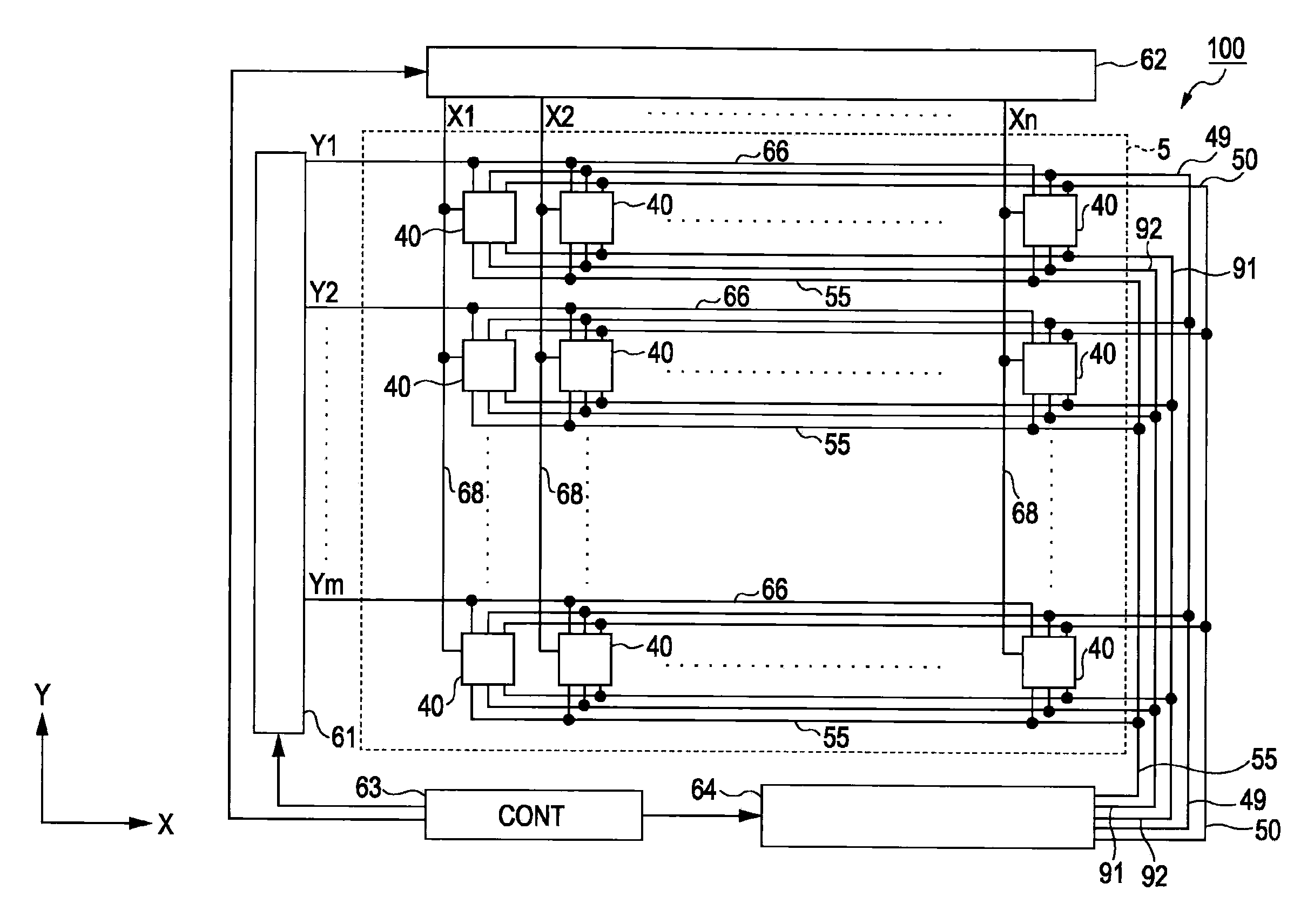
[0063]FIG. 1 is a schematic diagram showing the configuration of an electrophoretic display device 100 according to an embodiment of the invention.

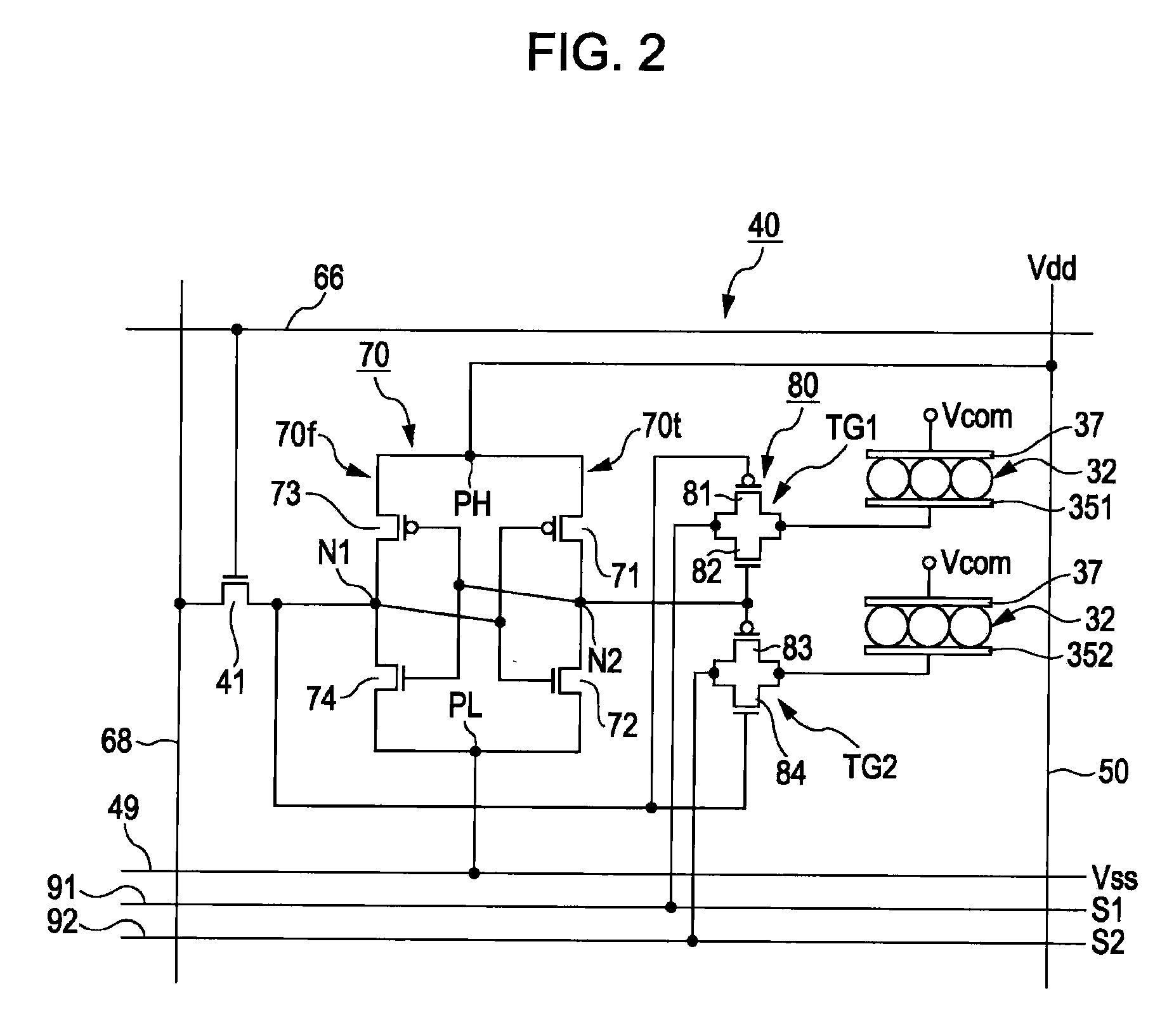
[0064]The electrophoretic display device 100 includes a display unit 5 in which a plurality of pixels 40 is arranged. In the periphery of the display unit 5, a scanning line driving circuit 61, a data line driving circuit 62, a controller (control unit) 63, and a c...


PUM

PropertyMeasurementUnit
electric potentialaaaaaaaaaa
leakage currentsaaaaaaaaaa

Abstract

An electrophoretic display device includes a first substrate and a second substrate that face each other, an electrophoretic element disposed between the first substrate and the second substrate, the electrophoretic element including electrophoretic particles, a display unit that has a plurality of pixels including the electrophoretic element, a common electrode that is formed on an electrophoretic element side of the second substrate, and a first control line and a second control line that are formed in either the first substrate or the second substrate. Each of the plurality of pixels includes a pixel switching element, a memory circuit that is connected to the pixel switching element, a switching circuit that is connected to the memory circuit, and a first pixel electrode and a second pixel electrode that are connected to the switching circuit and are disposed to face the common electrode. The switching circuit includes a first switch that controls a conductive state between the first control line and the first pixel electrode in accordance with an output signal of the memory circuit and a second switch that controls a conductive state between the second control line and the second pixel electrode in accordance with the output signal of the memory circuit.

Description

BACKGROUND[0001]1. Technical Field[0002]The present invention relates to an electrophoretic display device and an electronic apparatus.[0003]2. Related Art[0004]As electrophoretic display devices of an active matrix type, devices having a switching transistor and a memory circuit (SRAM: static random access memory) within each pixel have been known (see US 2008 / 0238867). Furthermore, the applicant of the invention has proposed an electrophoretic display device in which a switching circuit is disposed within a pixel in addition to the memory circuit (see US 2008 / 0238867).[0005]FIG. 16A is a circuit diagram of a pixel 540 of an electrophoretic display device 500 having the above-described configuration disclosed in US 2008 / 0238867. FIG. 16B is a schematic cross-section view of a display unit 505 of the electrophoretic display device 500.[0006]As shown in FIG. 16A, the pixel 540 includes a selection transistor 41, a latch circuit 70, a switching circuit 580, a pixel electrode 35, an el...

Claims


Application Information

Patent Timeline
Patent Type & Authority Applications(United States)
IPC IPC(8): G09G3/34G02F1/167G02F1/16757
CPCG02F1/167G09G3/2074G09G3/344G09G2300/0443G09G2300/0814G09G2330/021G09G2310/0262G09G2310/04G09G2320/0209G09G2320/043G09G2300/0857G02F1/16757G02F1/1685
Inventor MURAYAMA, TETSUROSHIMODAIRA, YASUHIROMAEDA, HIROSHI
Owner E INK CORPORATION
Why Eureka
Try Eureka