System and method for processing substrates with detachable mask

a technology of substrates and masks, applied in the field of substrate processing, can solve the problems of increasing the time and cost of fabricating semiconductor circuits, and the problem of particularly problematic problems

Active Publication Date: 2010-01-07
INTEVAC
View PDF22 Cites 26 Cited by
  • Summary
  • Abstract
  • Description
  • Claims
  • Application Information

AI Technical Summary

Benefits of technology

[0013]According to another aspect of the invention, the mask is used in an etch processing, for example, to avoid or repair edge shunt. According to one embodiment, the mask is made of a solid material having the shape of the substrate, but having a circumference that is a bit smaller from the substrate's circumference. The mask is placed over the substrate and etch is performed over the mask using, e.g. plasma or ion beam. Since the mask covers most of the substrate, the ion beam or plasma will cause etching of only the circumference of the substrate, thereby removing the top conductive layer about the circumference of the substrate. Consequently, edge shunt is avoided.

Problems solved by technology

It should be appreciated that the use of such masks, while indispensable in the semiconductor art, dramatically increases the time and costs of fabricating semiconductor circuits.
This problem is especially problematic with CIGS thin film solar cells.

Method used


Image

  • System and method for processing substrates with detachable mask
  • System and method for processing substrates with detachable mask
  • System and method for processing substrates with detachable mask

Examples


Embodiment Construction

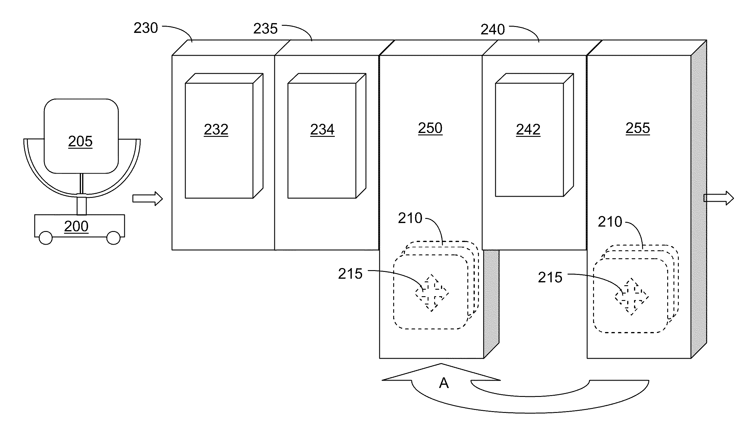
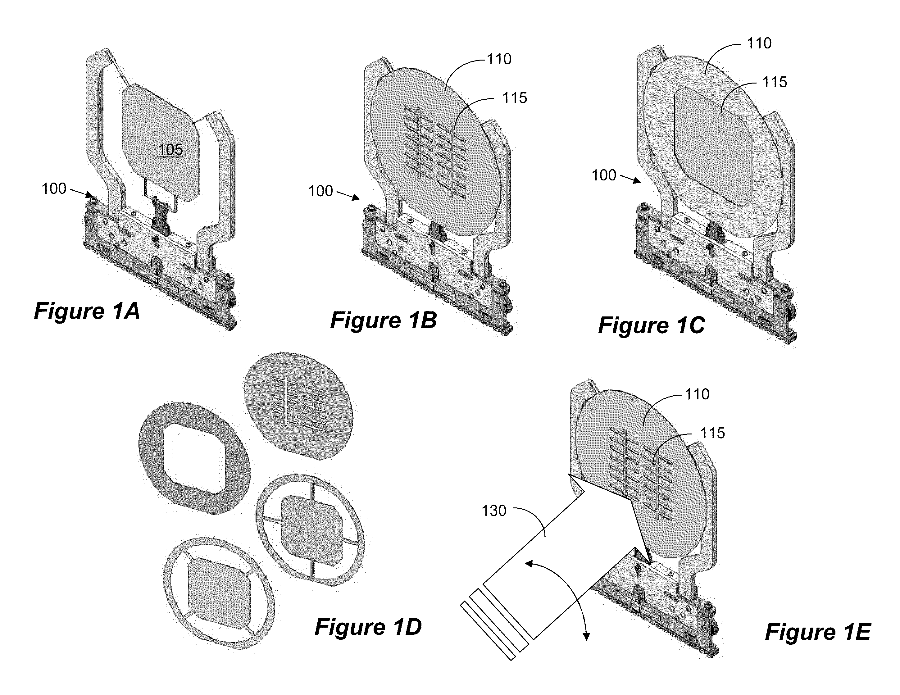
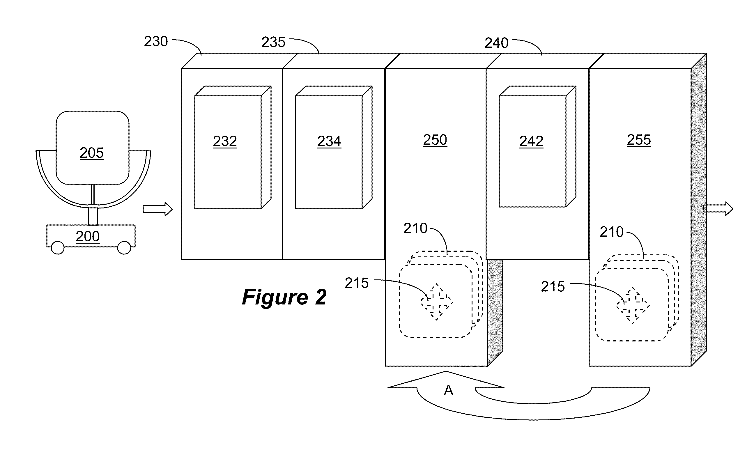
[0027]A detailed description will now be given of embodiments of the invention for enabling substrate processing using detachable masks. Such processing is particularly advantageous for solar cell fabrication. FIG. 1A is a perspective view of a substrate carrier 100 with a pseudo square substrate 105 without a mask present. In this particular example, the next processing step is to form a patterned layer over the surface of the substrate 105. For this purpose, a patterned mask is loaded onto the carrier in close proximity or actually touching the surface of the substrate. An example of a carrier with a patterned mask is depicted in FIG. 1B. In this example, the carrier 100 holds a pseudo square substrate 105 (obscured from view by the mask) and a trace mask 110 having a circuit pattern 115 carved out therein. The mask 110 is made of, for example, a 400 series stainless steel of 0.03″ thickness. Once the mask 110 is loaded, the carrier is transferred into a sputtering chamber and spu...


PUM

PropertyMeasurementUnit
vacuum environmentaaaaaaaaaa
mechanical mechanismaaaaaaaaaa
magneticaaaaaaaaaa

Abstract

Apparatus and methods are provided that enable processing of patterned layers on substrates using a detachable mask. Unlike prior art where the mask is formed directly over the substrate, according to aspects of the invention the mask is made independently of the substrate. During use, the mask is positioned in close proximity or in contact with the substrate so as to expose only portions of the substrate to processing, e.g., sputtering or etch. Once the processing is completed, the mask is moved away from the substrate and may be used for another substrate. The substrate may be cycled for a given number of substrates and then be removed for cleaning or disposal.

Description

RELATED APPLICATIONS[0001]This application claims priority benefit from U.S. provisional applications Ser. Nos. 61 / 077,054 and 61 / 176,003, filed on Jun. 30, 2008 and May 6, 2009, respectively, the entire disclosure of which is incorporated herein by reference.BACKGROUND[0002]1. Field[0003]The subject invention relates to processing of substrates, especially for processing substrates fabricated to operates as photovoltaic cells.[0004]2. Related Art[0005]Substrate processing tools are used to make hard-drive disks, semiconductor computer chips, solar panels, and the like, from substrates made of materials such as semiconductor wafers, glass, stainless steel, etc. Typically, the substrate processing tools includes several substrate chambers that perform various processes that modify the substrate, such as, deposition, cleaning, etch, heat / cool, etc. While in the semiconductor fabrication field the various processing steps, such as deposition and etch, are performed on only selected par...

Claims


Application Information

Patent Timeline
Patent Type & Authority Applications(United States)
IPC IPC(8): H01L21/308C23C14/34C23F4/00C23F1/08C23C14/50H01L21/3065
CPCH01L21/67069H01L21/67173H01L21/67207H01L21/67346H01L21/67712H01L31/18H05K3/143
Inventor BARNES, MICHAEL S.BLUCK, TERRY
Owner INTEVAC
Why Eureka
Try Eureka