Sensor device and method of operating the same

Inactive Publication Date: 2010-01-14
ATLAB INC
View PDF6 Cites 0 Cited by
  • Summary
  • Abstract
  • Description
  • Claims
  • Application Information

AI Technical Summary

Benefits of technology

[0029]As a consequence, a sensor device according to the present invention enables serial communication of data between semiconductor devices so that the number of connection lines can be lessened and the minimum data size required for the communication of data between the semiconductor devices can be reduced.

Problems solved by technology

As described above, a conventional sensor device has become problematic in that all touch sense signal generators 100-1 to 100-N should transmit position information to the host computer 120 irrespective of whether or not each of the touch sense signal generators 100-1 to 100-N generates a touch signal.

Method used


Image

  • Sensor device and method of operating the same
  • Sensor device and method of operating the same
  • Sensor device and method of operating the same

Examples


Embodiment Construction

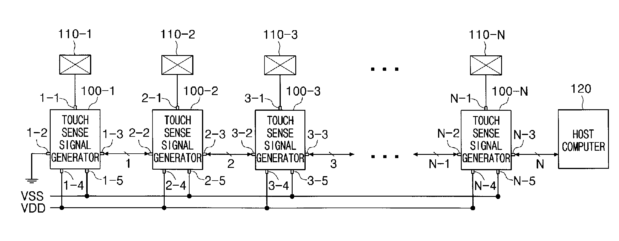
[0039]A sensor device and a method of operating the same according to the present invention will now be described more fully hereinafter with reference to the accompanying drawings, in which exemplary embodiments of the invention are shown.

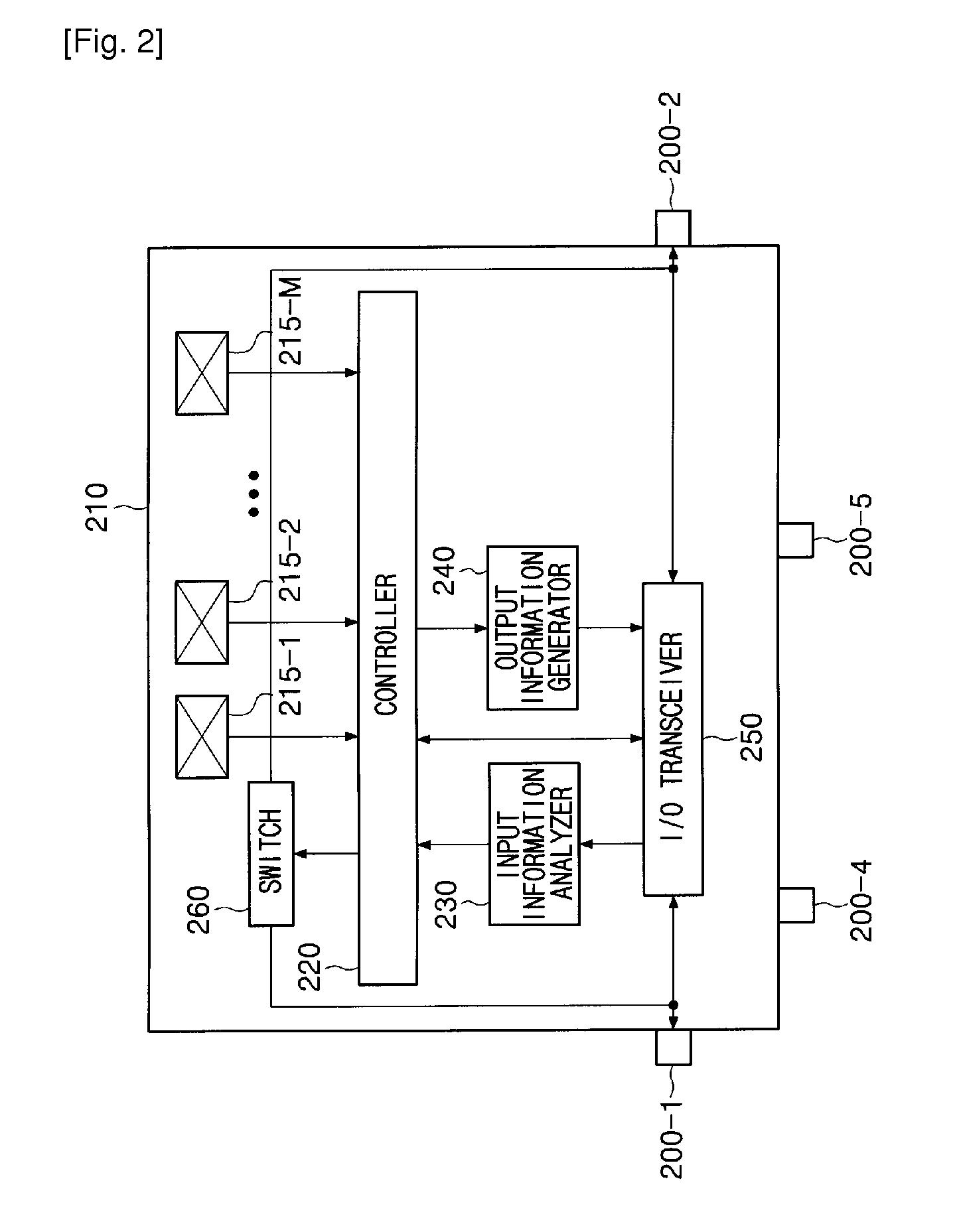
[0040]FIG. 2 is a diagram showing the construction of a semiconductor device included in a sensor device according to an exemplary embodiment of the present invention.

[0041]A semiconductor device 210 according to the present invention includes input / output (I / O) terminals 200-1 and 200-2, a power supply voltage terminal 200-4 connected to a power supply voltage VDD, and a ground voltage terminal 200-5 connected to a ground voltage VSS, which are external data I / O terminals, as in FIG. 1. The semiconductor device 210 includes a touch pad 215-1 to 215-M, a controller 220, an input information analyzer 230, an output information generator 240, an I / O transceiver 250, and a switch 260. An I / O controller communicating with an external semiconductor dev...


PUM


Abstract

Provided are a sensor device and a method of operating the same. The sensor device includes a plurality of semiconductor devices connected in series. When a semiconductor device does not sense a state of contact with an object and receives first sensing data from a preceding semiconductor device, the semiconductor device outputs the first sensing data to a succeeding semiconductor device. When the semiconductor device senses the state of contact with the object and receives the first sensing data from the preceding semiconductor device, the semiconductor device generates second sensing data and outputs the first and second sensing data to the succeeding semiconductor device. When the semiconductor device senses the state of contact with the object and does not receive the first sensing data from the preceding semiconductor device, the semiconductor device generates the second sensing data and outputs the second sensing data to the succeeding semiconductor device. The method includes the steps of: generating, by at least one semiconductor device for generating a sense signal, identification (ID) information, storing and outputting the ID information to the succeeding semiconductor device after a supply voltage is initially applied to the semiconductor device; outputting first sensing data to the succeeding semiconductor device when a state of contact with an object is not sensed and the first sensing data is received from a preceding semiconductor device; generating second sensing data when the state of contact with the object is sensed, and outputting the first sensing data and the second sensing data when the first sensing data is received from the preceding semiconductor device; and outputting the second sensing data when the first sensing data is not received from the preceding semiconductor device.

Description

TECHNICAL FIELD[0001]The present invention relates to a sensor device and a method of operating the same and, more particularly, to a sensor device and a method of operating the same, which can reduce the size of data transmitted and received between two or more semiconductor devices.BACKGROUND ART[0002]A sensor system of an electronic device includes a plurality of input channels (i.e., a buttons or touch pads) and touch sense signal generators. Each of touch sense signal generators is connected to at least one input channel to generate a touch sense signal. Thus, the sensor system transmits the touch sense signal to a host computer to recognize externally input touch information. In this case, the touch sense signal generators are connected in a daisy-chain manner, which is a kind of serial connection method, to effectively transmit and receive touch signals and other information.[0003]FIG. 1 is a block diagram showing a conventional communication method used to connect touch sens...

Claims


Application Information

Patent Timeline
IPC IPC(8): G06F3/041
CPCG06F3/041G06F3/04166G06F3/038G06F13/14G06F13/4247
Inventor LEE, JEI-HYUKLEE, BANG-WONSHIN, YOUNG-HOHONG, JAE-SURK
Owner ATLAB INC
Why Eureka
Try Eureka