Ceramic printed circuit board (PCB) and inkjet printhead assembly using the same

Inactive Publication Date: 2010-01-14
HEWLETT PACKARD DEV CO LP
View PDF4 Cites 2 Cited by
  • Summary
  • Abstract
  • Description
  • Claims
  • Application Information

AI Technical Summary

Benefits of technology

[0008]The present general inventive concept provides a ceramic printed circuit board (PCB) which includes a termination resistor capable of being located at a minimum distance from a final reception terminal, in order to prevent the signal quality from being reduced, and an inkjet printhead assembly using the ceramic PCB.
[0021]The foregoing and / or other features and utilities of the present general inventive concept may be achieved by providing a printed circuit board including a final reception terminal, a circuit pattern unit to transmit a received signal to the final reception terminal, and a termination resistor electrically connected to the circuit pattern unit and formed to reduce a distortion of the received signal.
[0025]The foregoing and / or other features and utilities of the present general inventive concept may be achieved by providing a printed circuit board, including a termination resistor disposed between a plurality of circuit patterns to reduce a distortion of a signal received and communicated by the plurality of circuit patterns, and a final reception terminal to finally receive the signal communicated by the plurality of circuit patterns.

Problems solved by technology

However, if a termination resistor is mounted in a ceramic board, the termination resistor may be electrically connected to a head chip via a pad, so signal shorts may occur due to leakage of ink.
However, to remove these problems, if the termination resistor is mounted in a main board, the distance between the termination resistor and the head chip may increase, so the LVDS may be distorted as illustrated in FIG. 1. FIGS. 1 and 2 illustrate graphs of signal quality measured when a conventional termination resistor is mounted in a main board.

Method used


Image

  • Ceramic printed circuit board (PCB) and inkjet printhead assembly using the same
  • Ceramic printed circuit board (PCB) and inkjet printhead assembly using the same
  • Ceramic printed circuit board (PCB) and inkjet printhead assembly using the same

Examples


Embodiment Construction

[0046]Reference will now be made in detail to exemplary embodiments of the present general inventive concept, with reference to the accompanying drawings, wherein like reference numerals refer to the like elements throughout. The embodiments are described below in order to explain the present general inventive concept by referring to the figures.

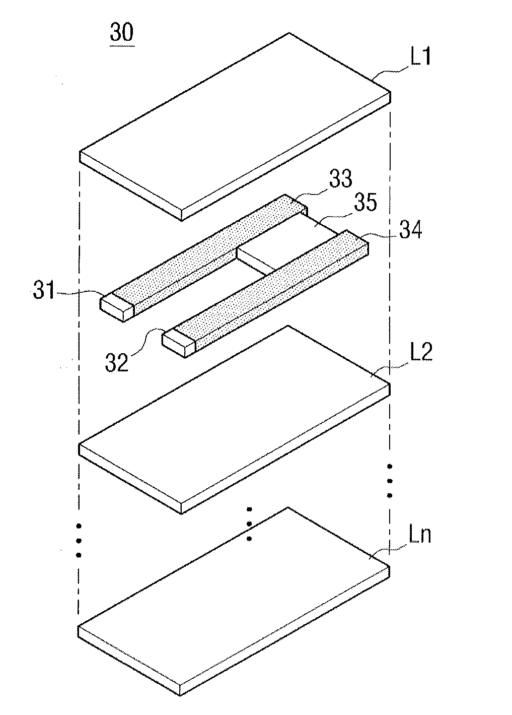
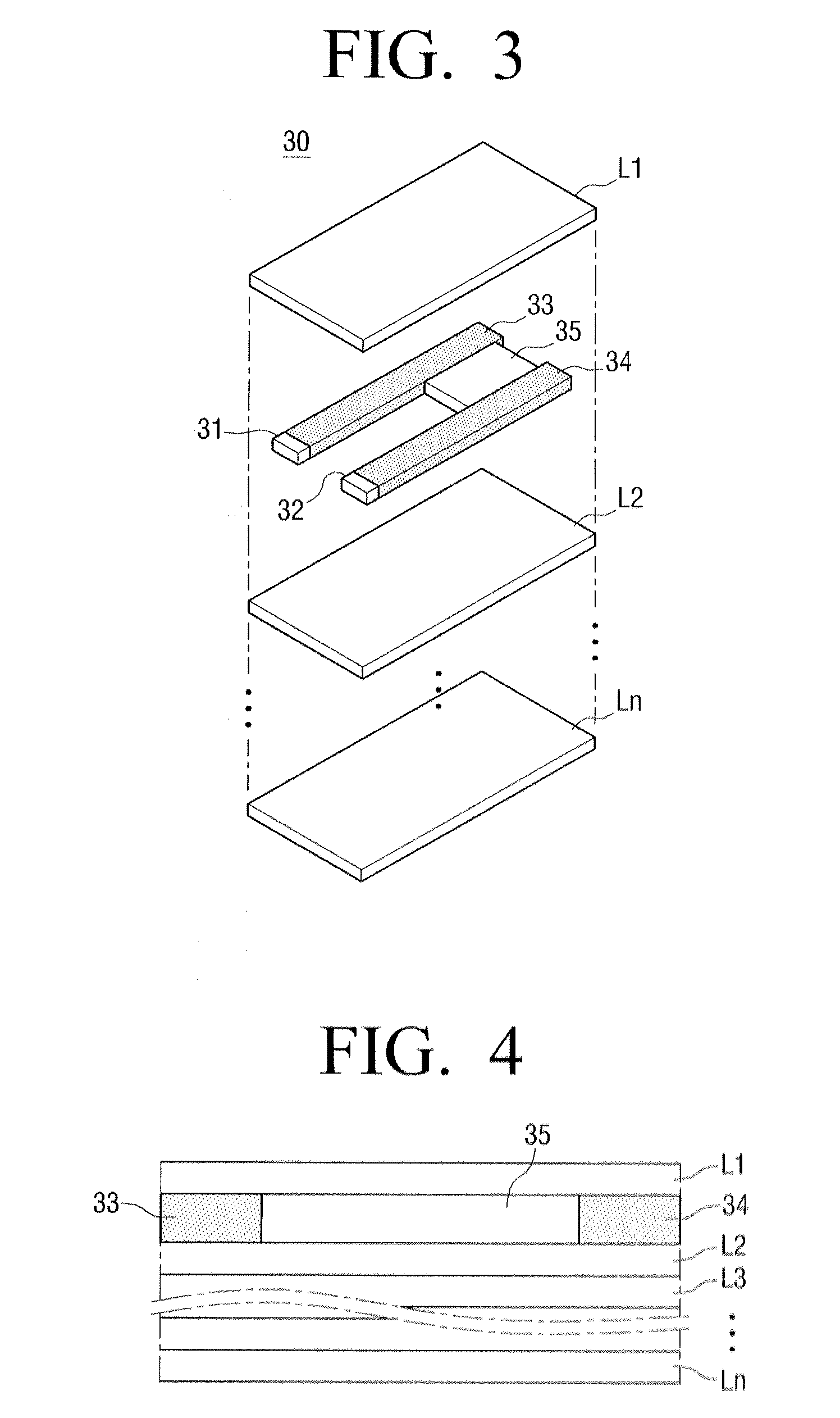
[0047]FIG. 3 illustrates a ceramic printed circuit board (PCB) 30 according to an exemplary embodiment of the present general inventive concept, and FIG. 4 illustrates a partial side view of the ceramic PCB 30.

[0048]Referring to FIGS. 3 and 4, the ceramic PCB 30 includes a plurality of layers L1, L2, . . . , Ln (here, n is a positive integer), a plurality of terminals 31, 32, a plurality of circuit patterns 33, 34, and a termination resistor 35.

[0049]The plurality of layers L1, L2, . . . , Ln are stacked to form the ceramic PCB 30. The plurality of layers L1, L2, . . . , Ln includes insulating layers made of, for example, ceramic. The use of...


PUM


Abstract

A ceramic printed circuit board (PCB) and an inkjet printhead assembly using the ceramic PCB. A ceramic PCB in which a plurality of layers are stacked includes a plurality of terminals to receive an electric signal from an external source, a plurality of circuit patterns connected to the plurality of terminals to transmit the electric signal, and a termination resistor having a predetermined thickness disposed between the plurality of circuit patterns, wherein the termination resistor is mounted between the plurality of stacked layers.

Description

CROSS-REFERENCE TO RELATED APPLICATIONS[0001]This application claims priority under 35 U.S.C. §119(a) from Korean Patent Application No. 10-2008-0066011, filed on Jul. 8, 2008, in the Korean Intellectual Property Office, the disclosure of which is incorporated herein by reference in its entirety.BACKGROUND OF THE INVENTION[0002]1. Field of the Invention[0003]The present general inventive concept relates to a ceramic printed circuit board (PCB) and an inkjet printhead assembly. More particularly, the present general inventive concept relates to a ceramic PCB which includes a termination resistor to increase signal quality, and an inkjet printhead assembly using the ceramic PCB.[0004]2. Description of the Related Art[0005]Inkjet printers transmit low voltage differential signaling (LVDS) generated by drivers of main boards to head chips, namely final reception terminals, so that ink is ejected from the head chips. In order to increase signal quality, it is desirable that termination r...

Claims


Application Information

Patent Timeline
IPC IPC(8): B41J2/14H05K1/02H01P1/24
CPCB41J2/14B41J2002/14491H01P1/268H05K2203/1453H05K1/0306H05K1/167H05K1/0237B41J2/14129B41J2/1643B41J2/04541H01L2224/32225
Inventor LEE, JUN-HOJEON, SEONG-NAM
Owner HEWLETT PACKARD DEV CO LP
Why Eureka
Try Eureka