Semiconductor device

a technology of semiconductor devices and memory lsi, applied in the direction of semiconductor/solid-state device details, solid-state devices, printed circuit structure associations, etc., can solve problems such as no solutions, and achieve the effect of improving system performance and improving communication between memory lsi and logic lsi

Inactive Publication Date: 2010-01-14
HITACHI LTD
View PDF8 Cites 84 Cited by
  • Summary
  • Abstract
  • Description
  • Claims
  • Application Information

AI Technical Summary

Benefits of technology

[0013]According to the present invention, the performance of communication between a memory LSI and a logic LSI and b

Problems solved by technology

The applicant has found a problem that the conventional simple stacking of logic LSIs and memory LSIs requires ensuring heat dissipation for increasing heat density and ensuring an adequate transmission path characteristi

Method used


Image

  • Semiconductor device
  • Semiconductor device
  • Semiconductor device

Examples


Embodiment Construction

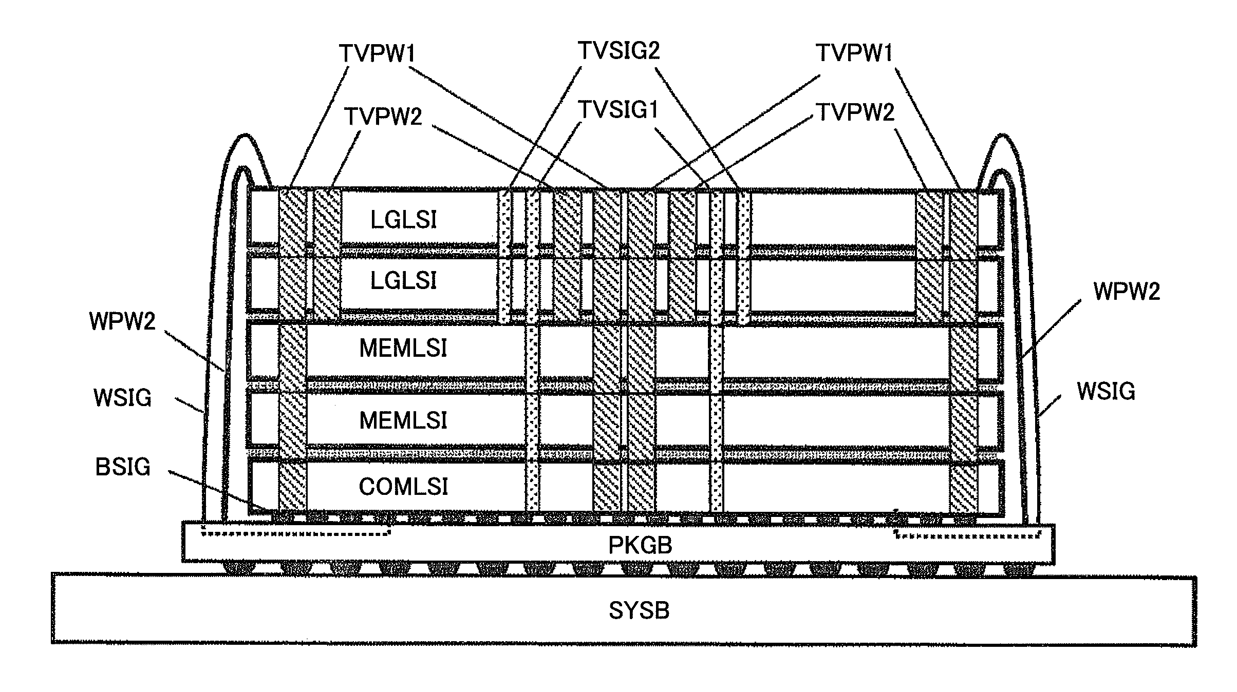
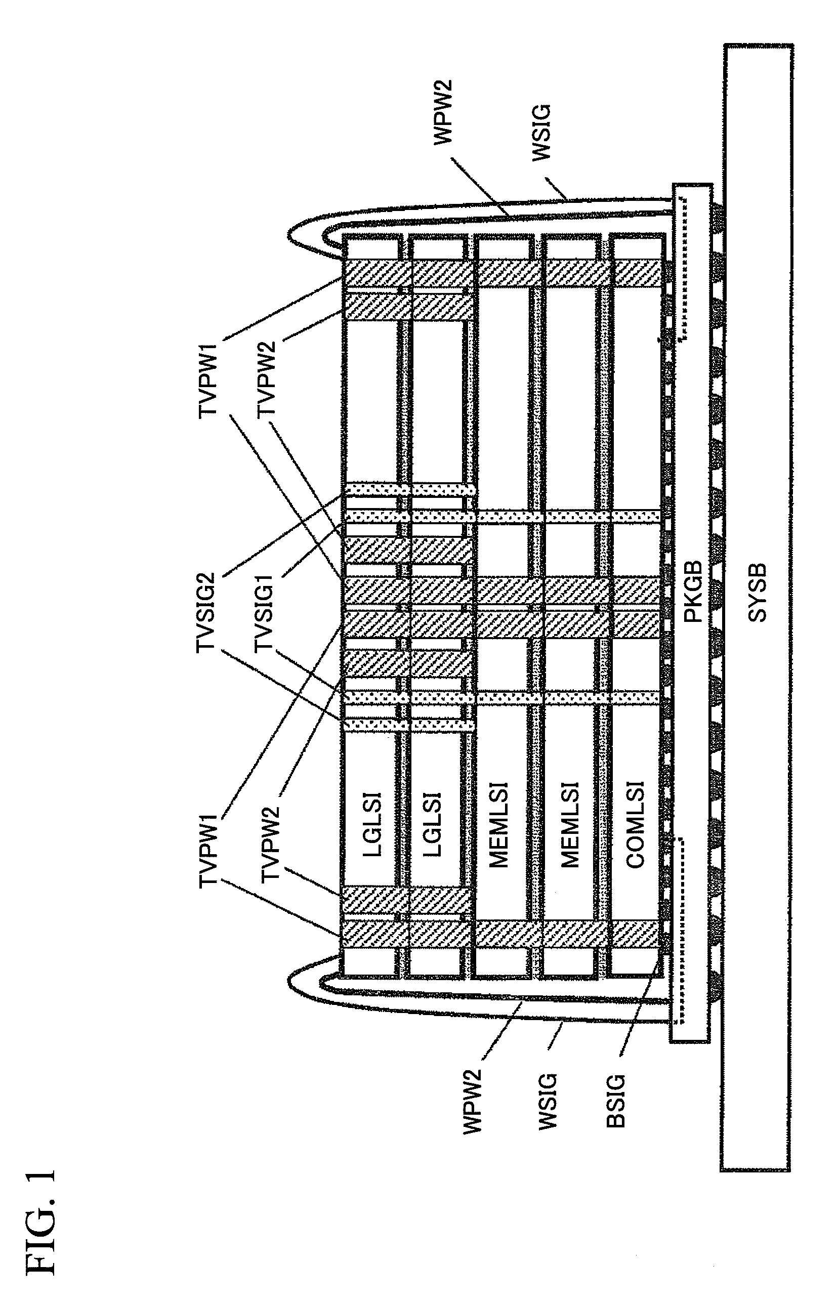
[0028]FIG. 1 shows one embodiment of stacked LSIs. A cross section of the stacked LSIs is shown. In the present embodiment, an external-communication LSI (COMLSI) is stacked on a package board PKGB, two memory LSIs (MEMLSIs) storing data are stacked on the external-communication LSI, and two logic LSIs (LGLSIs) including computing units are stacked on the upper memory LSI. The external-communication LSI includes a circuit that performs fast wired communication with a component on a system board that is outside the stacked-LSI package at a communication frequency exceeding 1 GHz. Fast communication with the outside of the stacked-LSI package is performed through the external-communication LSI. The external-communication LSI is flip-connected to the package board with its circuitry / wiring surface being faced to the package board. The memory LSIs may be memories such as DRAMs, SRAMs, flash memories, magnetic memories. The logic LSIs may be general-purpose processors such as CPUs, speci...


PUM


Abstract

Traffic between logic LSIs and memory is increasing year by year and there is demand for increase of capacity of communication between them and reduction of power consumption in the communication. Communication distances between LSIs can be reduced by stacking the LSIs. However, in a simple stack of logic LSIs and memory LSIs, it is difficult to ensure heat dissipation to cope with increasing heat densities and ensure transmission characteristics for fast communication with the outside of the stacked package. Also required is a connection topology that improves the performance of communication among the stacked LSIs while ensuring the versatility of the LSIs. An external-communication LSI, a memory LSI, and a logic LSI are stacked in this order in a semiconductor package and are interconnected by through silicon vias. Output terminals of multiple stacked LSIs are connected to an input terminal of a through silicon via of the stacked memory LSI and input terminals of multiple stacked LSIs are connected to an output terminal of a through silicon via of the stacked memory LSI, thereby directly connecting both of the external-communication LSI and the logic LSI to a wiring line of the memory LSI.

Description

CLAIM OF PRIORITY[0001]The present application claims priority from Japanese patent application JP 2008-179704 filed on Jul. 10, 2008, the content of which is hereby incorporated by reference into this application.BACKGROUND OF THE INVENTION[0002]1. Field of the Invention[0003]The present invention relates to stacked LSIs.[0004]2. Background Art[0005]Performances of LSIs have been improved by integrating more and more transistors on one chip with the advance of the microfabrication technology. However, it will not necessarily be an optimum solution to increase the number of transistors integrated on one chip as before, because of the limitations of miniaturization and increase in cost of using cutting-edge processes. Therefore, three-dimensional integration in which multiple LSIs are stacked will be promising technology.[0006]In such 3D integration, communication capability among the stacked LSIs and between the stacked LSIs and an external device is important. As communication meth...

Claims


Application Information

Patent Timeline
IPC IPC(8): H05K1/14
CPCH01L23/481H01L2225/06531H01L25/18H01L2224/16145H01L2224/48227H01L2224/73257H01L2225/0651H01L2225/06513H01L2225/06517H01L2924/01033H01L2924/01082H01L2924/01094H01L2924/3011H01L24/48H01L2924/01006H01L2924/01023H01L24/73H01L2224/05573H01L2224/13025H01L2924/00014H01L2224/16225H01L2924/15311H01L2224/0554H01L2224/05599H01L2224/45099H01L2224/45015H01L2924/207H01L2224/0555H01L2224/0556
Inventor SAEN, MAKOTOOSADA, KENICHI
Owner HITACHI LTD
Why Eureka
Try Eureka