Pixel sensor cell with frame storage capability

Inactive Publication Date: 2010-01-21
GLOBALFOUNDRIES INC
View PDF15 Cites 24 Cited by
  • Summary
  • Abstract
  • Description
  • Claims
  • Application Information

AI Technical Summary

Benefits of technology

[0012]In the present invention, a set of frame transfer transistors are provided between a hold gate transistor and a transfer gate transistor of a CMOS image sensor to enable storage of charge generate in the photosensitive diode after exposure. The readout of the charges from the set of frame transfer transistors may be performed after a plurality of exposures of the CMOS image sensor, between each of whic

Problems solved by technology

For highly dynamic subjects (such as objects moving at a high rate of speed), the rolling shutter methodology can create image artifacts.
The global shutter method enables image capture of high speed subjects without image artifacts, but introduces a concern with the global shutter efficiency of the pixel since the integrity of the signal may be compromised by any charge leakage from the floating diffusion node between the time of the image capture and the time of the reading of the imager array.
Such a

Method used


Image

  • Pixel sensor cell with frame storage capability
  • Pixel sensor cell with frame storage capability
  • Pixel sensor cell with frame storage capability

Examples


Embodiment Construction

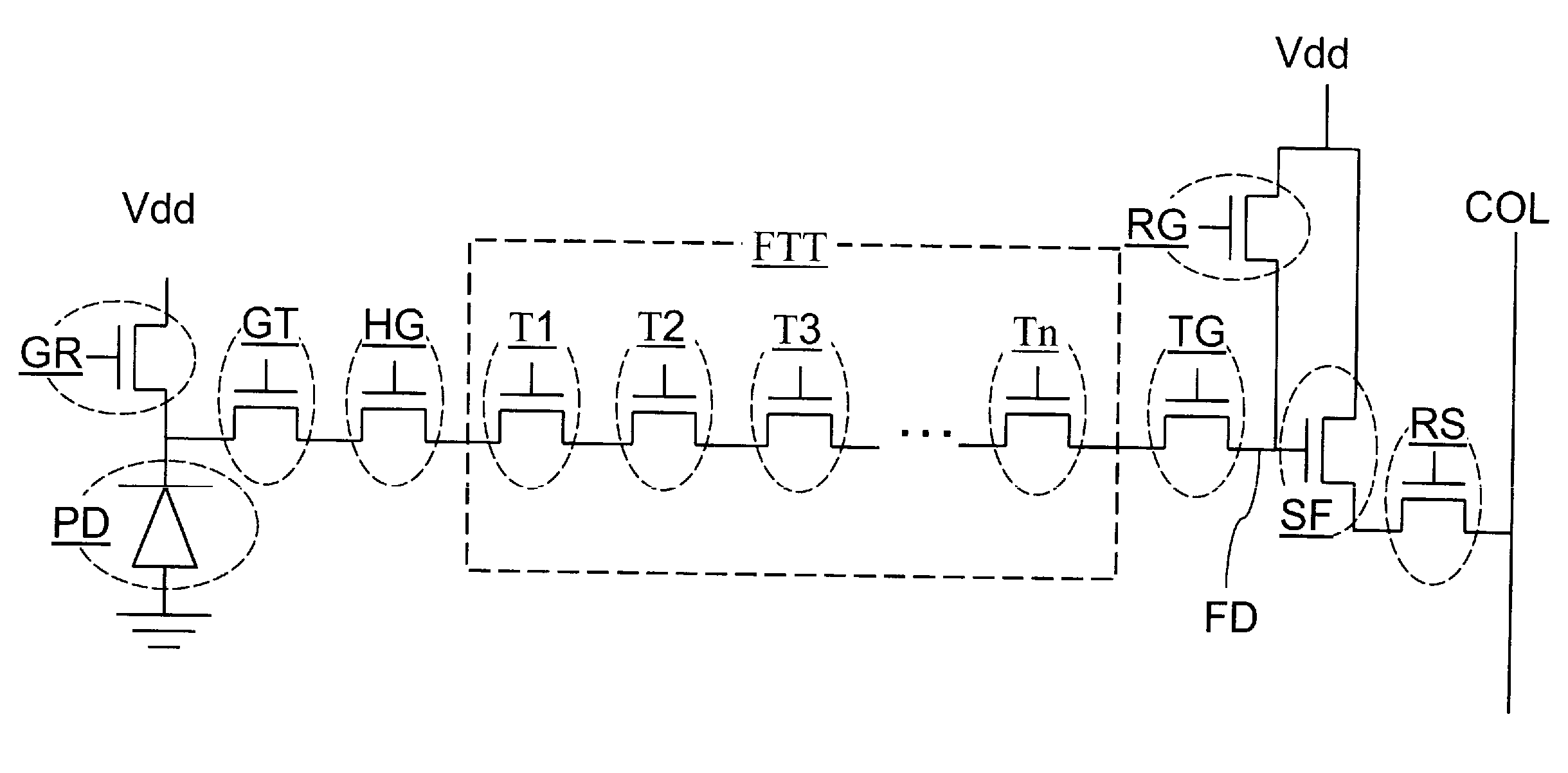
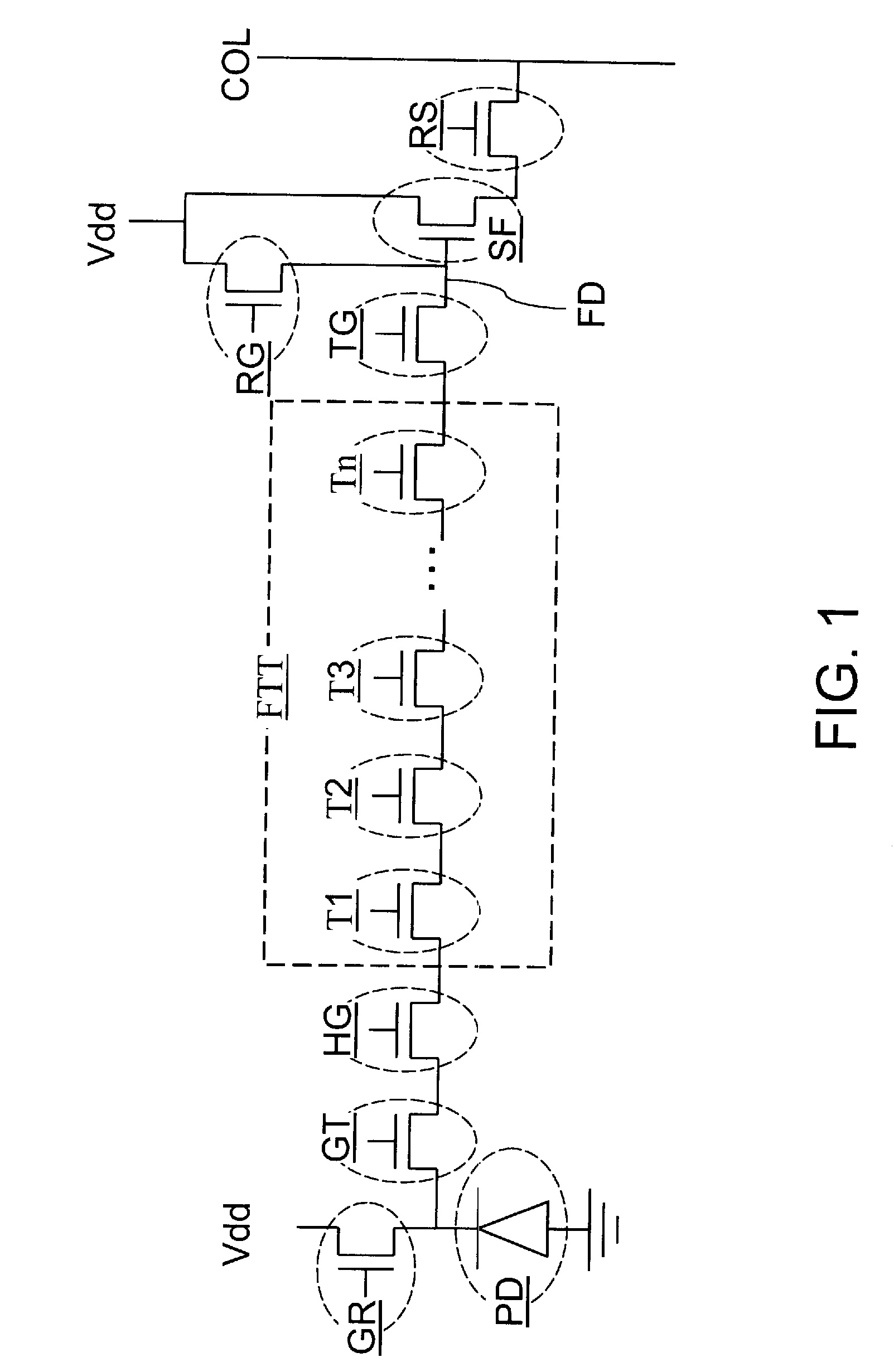
[0074]As stated above, the present invention relates to semiconductor circuits including a pixel sensor cell having the capability of storing frames prior to read out, and a design structure for the same, which are now described in detail with accompanying figures. As used herein, when introducing elements of the present invention or the preferred embodiments thereof, the articles “a”, “an”, “the” and “said” are intended to mean that there are one or more of the elements. Throughout the drawings, the same reference numerals or letters are used to designate like or equivalent elements. Detailed descriptions of known functions and constructions unnecessarily obscuring the subject matter of the present invention have been omitted for clarity. The drawings are not necessarily drawn to scale.

[0075]Referring to FIG. 1, a first exemplary semiconductor circuit comprising an image sensor pixel is shown according to the present invention. The first exemplary semiconductor circuit comprises a ...


PUM


Abstract

A set of frame transfer transistors are provided between a hold gate transistor and a transfer gate transistor of a CMOS image sensor to enable storage of charge generate in the photosensitive diode after exposure. The readout of the charges from the set of frame transfer transistors may be performed after a plurality of exposures of the CMOS image sensor, between each of which charges are shifted toward the transfer gate transistor within the set of frame transfer transistors. Useful operation modes are enabled including a burst mode operation for rapid capture of successive images and high dynamic range operations in which multiple images are taken with different exposure times or a large capacitance is provided by ganging the diffusions of the set of frame transfer transistors.

Description

RELATED APPLICATIONS[0001]The present application is related to co-pending U.S. application Ser. No. ______ (Attorney Docket No: BUR920080089US2; SSMP 22412), which is incorporated herein by reference.FIELD OF THE INVENTION[0002]The present invention relates to semiconductor circuits and semiconductor circuit design, and more particularly to semiconductor circuits including a pixel sensor cell having the capability of storing frames prior to read out, and a design structure for the same.BACKGROUND OF THE INVENTION[0003]A pixel sensor comprises an array of pixel sensor cells that detects two dimensional signals. Pixel sensors include image sensors, which may convert a visual image to digital data that may be represented by a picture, i.e., an image frame. The pixel sensor cells are unit devices for the conversion of the two dimensional signals, which may be a visual image, into the digital data. A common type of pixel sensors includes image sensors employed in digital cameras and opt...

Claims


Application Information

Patent Timeline
IPC IPC(8): H04N5/335
CPCH04N5/37452H04N5/2355H04N23/741H04N25/771
Inventor ADKISSON, JAMES W.ELLIS-MONAGHAN, JOHN J.KRISHNASAMY, RAJENDRANMULUGETA, SOLOMONMUSANTE, CHARLES F.RASSEL, RICHARD J.
Owner GLOBALFOUNDRIES INC
Why Eureka
Try Eureka