Method and structure for a CMOS image sensor using a triple gate process

a technology of cmos image sensor and triple gate process, which is applied in the direction of diodes, semiconductor devices, electrical equipment, etc., can solve the problems of high cost of integrated circuit or chip fabrication facilities, difficult devices, and limited process use, so as to achieve easy use and improve device reliability and performance. , the effect of high device reliability

Active Publication Date: 2010-01-21
SEMICON MFG INT (SHANGHAI) CORP
View PDF8 Cites 0 Cited by
  • Summary
  • Abstract
  • Description
  • Claims
  • Application Information

AI Technical Summary

Benefits of technology

[0010]Many benefits are achieved by way of the present invention over conventional techniques. For example, the present technique provides an easy to use process that relies upon conventional technology. In some embodiments, the method provides higher device reliability and performance. Depending upon the embodiment, one or more of these benefits may be achieved. These and other benefits will be described in more throughout the present specification and more particularly below.

Problems solved by technology

An integrated circuit or chip fabrication facility can cost hundreds of millions, or even billions, of U.S. dollars.
Making devices smaller is very challenging, as each process used in integrated fabrication has a limit.

Method used


Image

  • Method and structure for a CMOS image sensor using a triple gate process
  • Method and structure for a CMOS image sensor using a triple gate process
  • Method and structure for a CMOS image sensor using a triple gate process

Examples


Embodiment Construction

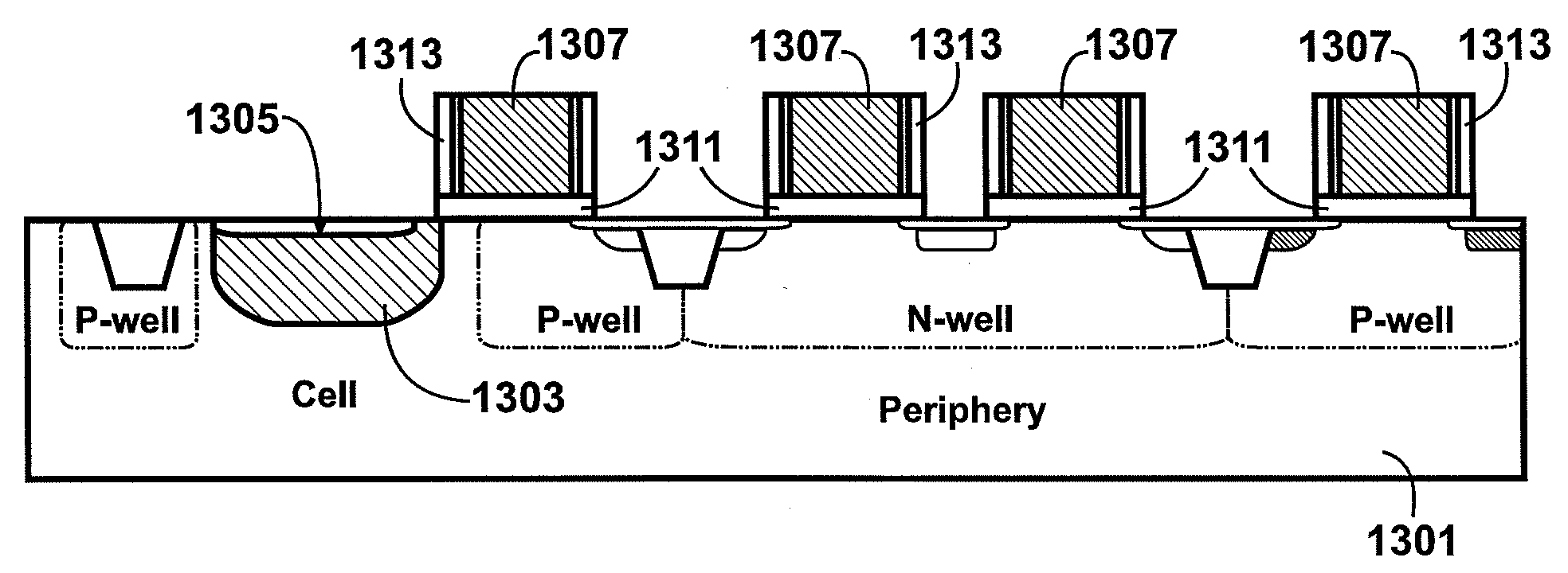
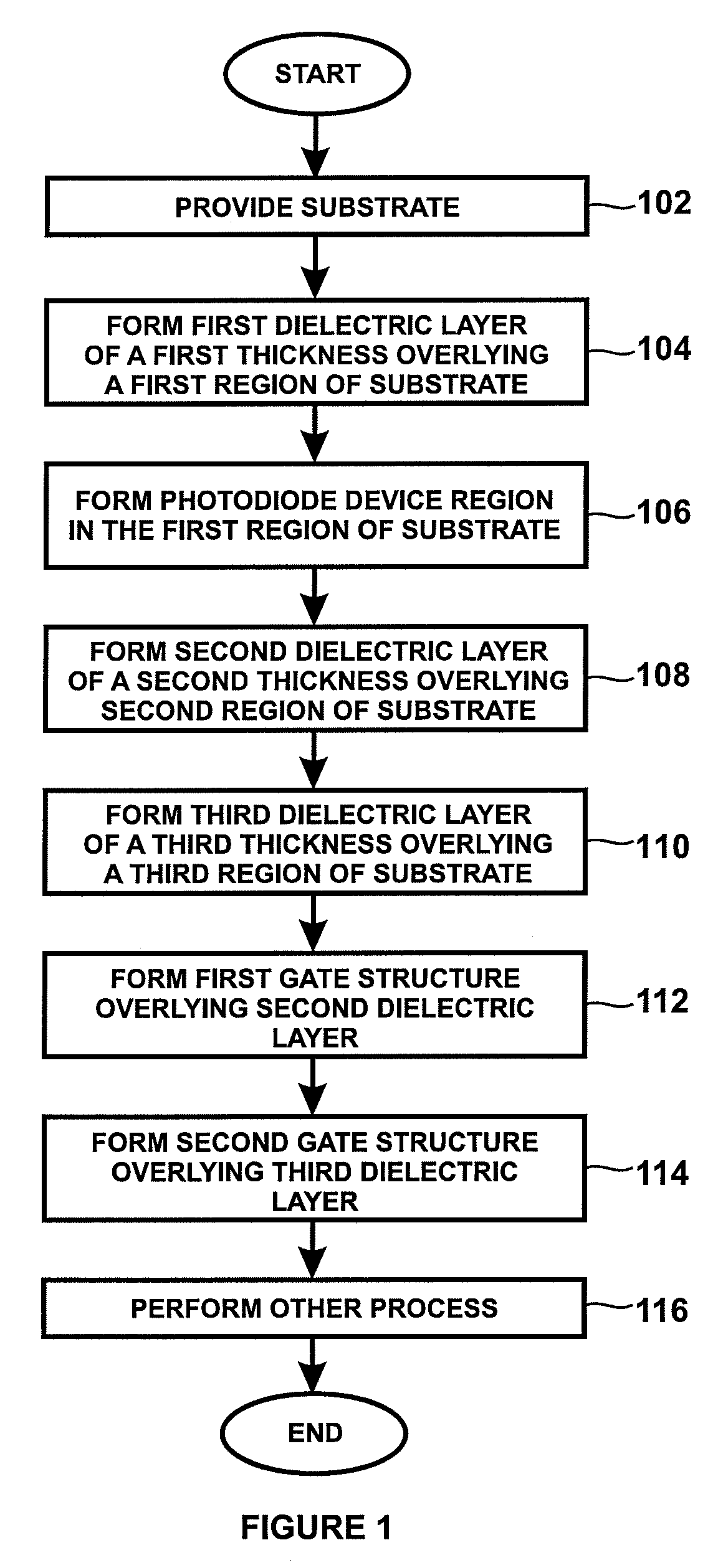
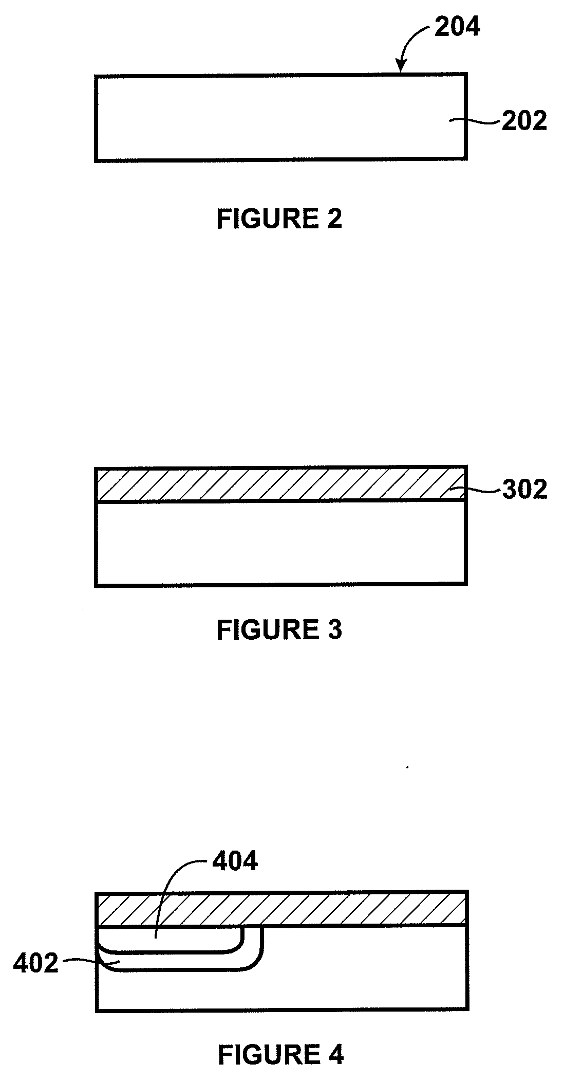
[0015]According to embodiments of the present invention, techniques for forming a CMOS image sensor is provided. In particular, embodiments according to the present invention provide techniques to form CMOS image sensor having a reduced leakage current. But it would be recognized that embodiments according to the present invention have a much broader range of applicability. For example, embodiments according to the present invention may be applied to forming other integrated circuit devices and others.

[0016]CMOS image sensors are emerging as a preferred technology for digital consumer applications. To enable improved pixel sensing performance, CMOS image sensor technology requires improved pixel layout design and integrated circuit processing. Dark current is a major factor influencing sensor performance especially under a low light condition. Factors that may contribute to dark current include defects on the silicon surface and silicon-gate oxide interface in photodiode regions and...


PUM


Abstract

A method of forming a CMOS image sensor device, the method includes providing a semiconductor substrate having a P-type impurity characteristic including a surface region. The method form a first thickness of silicon dioxide in a first region of the surface region, a second thickness of silicon dioxide in a second region of the surface region, and a third thickness of silicon dioxide in a third region of the surface region. The method includes forming a first gate layer overlying the second region and a second gate layer overlying the third region, while exposing a portion of the first thickness of silicon dioxide. An N-type impurity characteristic is formed within a region within a vicinity underlying the first thickness of silicon dioxide in the first region of the surface region to cause formation of a photo diode device characterized by the N-type impurity region and the P-type substrate.

Description

CROSS-REFERENCE TO RELATED APPLICATIONS[0001]This application claims priority to Chinese Application No. 200810040741.7, filed Jul. 15, 2008, commonly assigned, and incorporated herein by reference for all purposes.BACKGROUND OF THE INVENTION[0002]The present invention is directed to integrated circuits and their processing for the manufacture of semiconductor devices. More particularly, the invention provides a method and a structure for manufacturing a CMOS image sensor device having a reduced dark current characteristics for advanced application. But it would be recognized that the invention has a much broader range of applicability.[0003]Integrated circuits have evolved from a handful of interconnected devices fabricated on a single chip of silicon to millions of devices. Conventional integrated circuits provide performance and complexity far beyond what was originally imagined. In order to achieve improvements in complexity and circuit density (i.e., the number of devices capab...

Claims


Application Information

Patent Timeline
Patent Type & Authority Applications(United States)
IPC IPC(8): H01L31/18
CPCH01L27/14609H01L27/14689H01L27/14643
Inventor HUO, JIEGUANGYANG, JIANPING
Owner SEMICON MFG INT (SHANGHAI) CORP
Why Eureka
Try Eureka