Wafer Dicing Methods

Inactive Publication Date: 2010-01-21
TAIWAN SEMICON MFG CO LTD
View PDF6 Cites 51 Cited by
  • Summary
  • Abstract
  • Description
  • Claims
  • Application Information

AI Technical Summary

Benefits of technology

[0005]These and other problems are generally solved or circumvented, and technical advantages are generally achieved, by preferred embodiments of the present invention which provide improved wafer dicing methods of separating semiconductor dice on a semiconductor wafer. These methods include forming etch patterns between adjacent semiconductor dice to be separated. Various etch processes can be used to form the etch patterns. Th

Problems solved by technology

However, when used on wafers made of frangible semiconductor materials to divide semiconductor device dice of miniature die size, these known wafer dicing methods may not provide satisfactory results.
The method of mechanical cleaving and sawing leaves micro-cracks along the edges of the dicing cuts.
These cracks can easily propagate on a wafer through unexpected crack paths, which may lead to significant device damage and substantial device yield loss.
The effects of vibrating, shearing, and shocking accompanying a sawing operation may aggravate the cracking and create more device damages and yield losses.
Also, the physical dimension of a diamond saw blade limits the further scaling of the scribe lines on a semiconductor waf

Method used


Image

  • Wafer Dicing Methods
  • Wafer Dicing Methods
  • Wafer Dicing Methods

Examples


Embodiment Construction

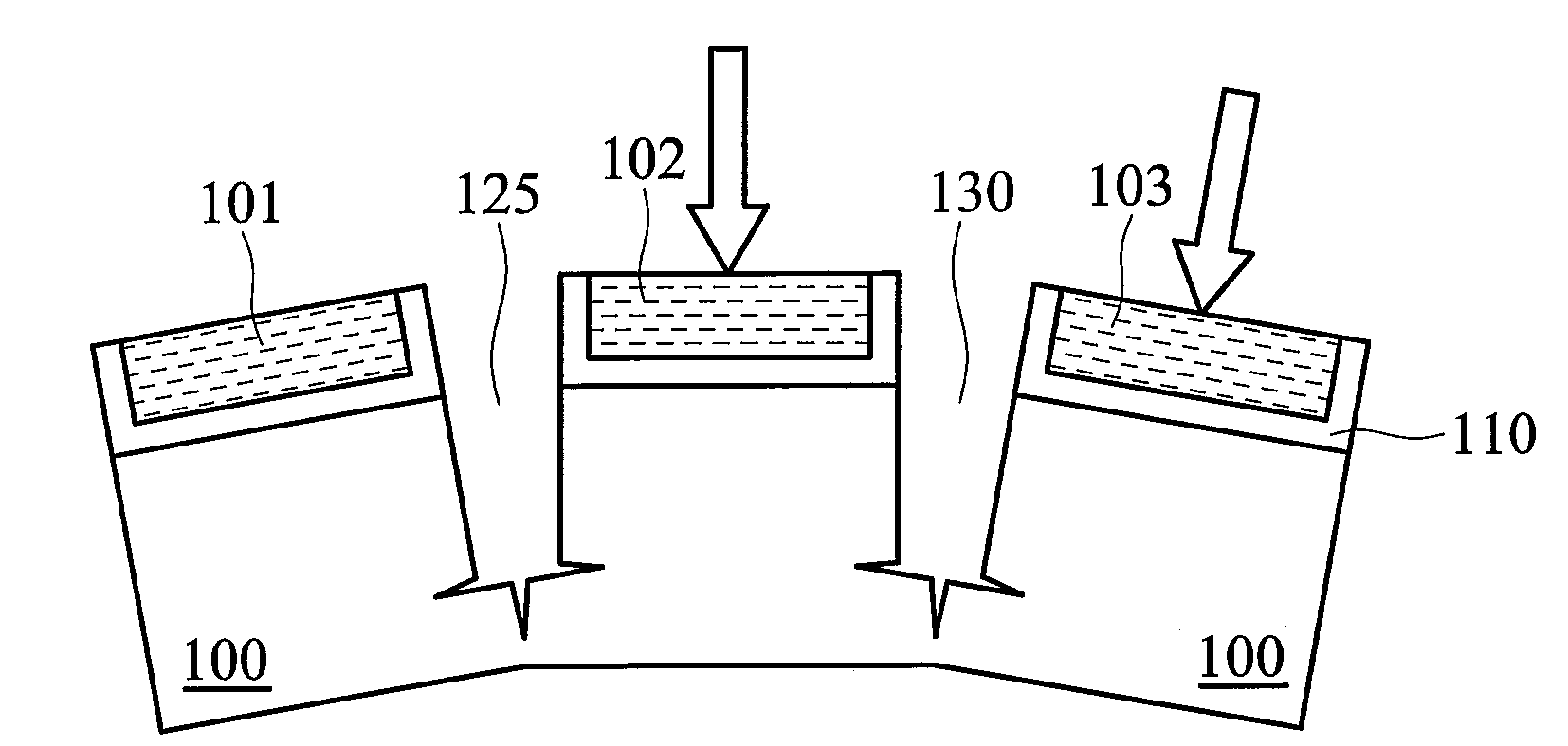
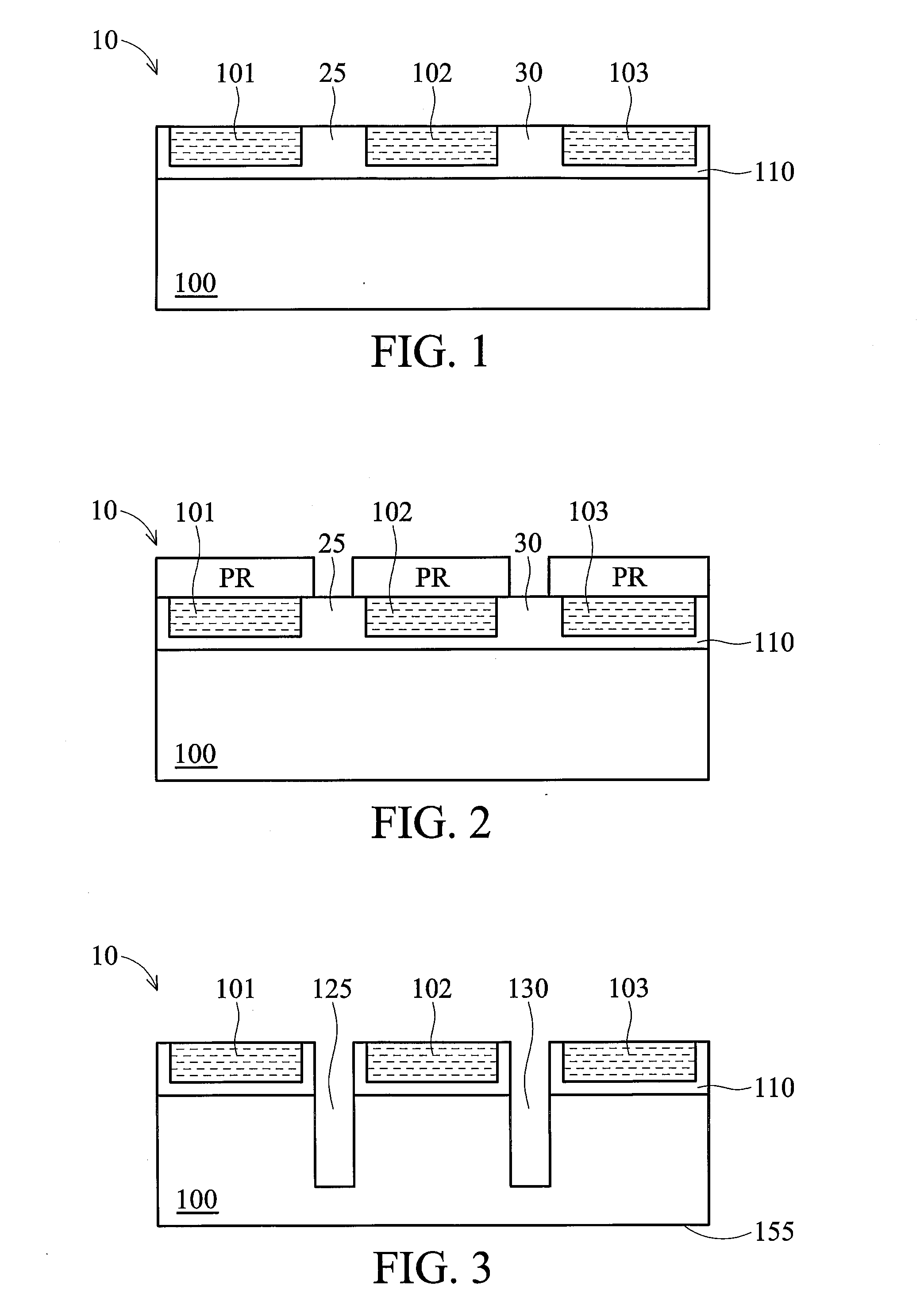
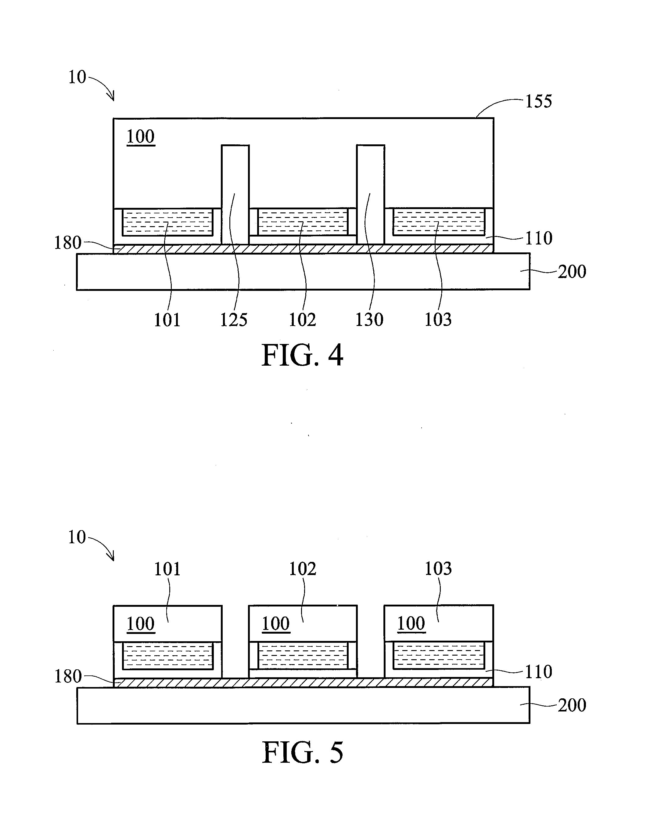
[0013]The making and using of the presently preferred embodiments are discussed in detail below. It should be appreciated, however, that the present invention provides many applicable inventive concepts that can be embodied in a wide variety of specific contexts. The specific embodiments discussed are merely illustrative of specific ways to make and use the invention, and do not limit the scope of the invention.

[0014]The present invention will be described with respect to preferred embodiments in a specific context, namely improved wafer dicing methods. The preferred embodiments may be used to separate a large diameter, frangible semiconductor wafer into dice having miniature die size. The preferred embodiments significantly ease the handing of the wafers to be separated, and may significantly alleviate or even eliminate the detrimental effects, such as micro-cracking and particle re-deposition associated with the conventional wafer dicing methods, therefore reducing the dicing-rela...


PUM


Abstract

Semiconductor wafer dicing methods are disclosed. These methods include forming etch patterns between adjacent semiconductor dice to be separated. Various etch processes can be used to form the etch patterns. The etch patterns generally reach a pre-determined depth into the wafer substrate significantly beyond the wafer top layer where pre-fabricated semiconductor dice are embedded. Semiconductor dice may be separated from a post-etch, large-sized, frangible wafer through wafer grinding, mechanical cleaving, and laser dicing approaches. Preferred embodiments result in reduced wafer-dicing related device damage and improved product yield.

Description

TECHNICAL FIELD[0001]The present invention relates generally to wafer dicing methods, and more particularly to methods of separating semiconductor wafers into chips.BACKGROUND[0002]Upon the completion of semiconductor manufacturing processes, a large number of duplicate semiconductor devices, such as light emitting diode (LED) devices are typically formed on a semiconductor wafer. These devices are separated by scribe lines on the processed wafer. Various techniques are employed to divide the processed wafers along the scribe lines into individual dice with each die representing a particular semiconductor device chip. Typical wafer dicing techniques adopted today include mechanical cleaving, laser dicing, and sawing with diamond blade.[0003]The method of mechanical cleaving involves pre-cracking a scribe line with a diamond tip and manually breaking the wafer along the scribe line, similar to the way a plate glass is cut for household purposes. The technique of laser dicing employs ...

Claims


Application Information

Patent Timeline
IPC IPC(8): H01L21/00
CPCH01L33/0095H01L21/78
Inventor YU, CHEN-HUACHIOU, WEN-CHIHCHEN, DING-YUAN
Owner TAIWAN SEMICON MFG CO LTD
Why Eureka
Try Eureka