Image sensor having nanodot

a nano-dot, image sensor technology, applied in the field of image sensors, can solve the problem of difficult focusing light onto a photoelectric conversion region using a micro-lens

Inactive Publication Date: 2010-01-28
SAMSUNG ELECTRONICS CO LTD
View PDF4 Cites 68 Cited by
  • Summary
  • Abstract
  • Description
  • Claims
  • Application Information

AI Technical Summary

Benefits of technology

[0021]The metal nanodot can have a size of a

Problems solved by technology

However, focusing light onto a photoelectric conversion region using the micro

Method used


Image

  • Image sensor having nanodot
  • Image sensor having nanodot
  • Image sensor having nanodot

Examples


Embodiment Construction

[0035]The present invention will now be described more fully with reference to the accompanying drawings in which example embodiments of the invention are shown. This invention may, however, be embodied in many different forms and should not be construed as limited to the exemplary embodiments set forth herein.

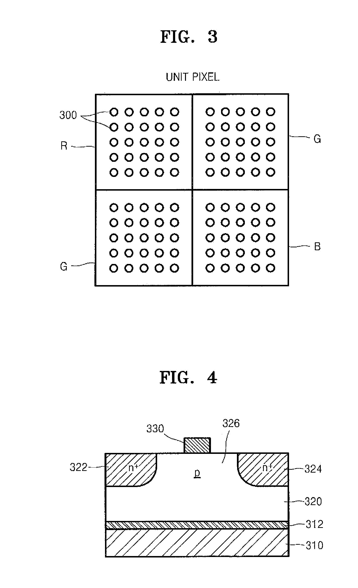
[0036]An image sensor according to an exemplary embodiment of the present invention includes a plurality of unit pixels arranged in an array. Each unit pixel includes a plurality of sub-pixels that respectively detect visible light having a predetermined wavelength. The sub-pixels may be a red pixel R, a green pixel G, or a blue pixel B. Color filters may be disposed on the sub-pixels. Each color filter selectively transmits light to be detected. A micro lens that focuses light may be disposed on the color filters.

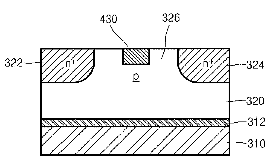
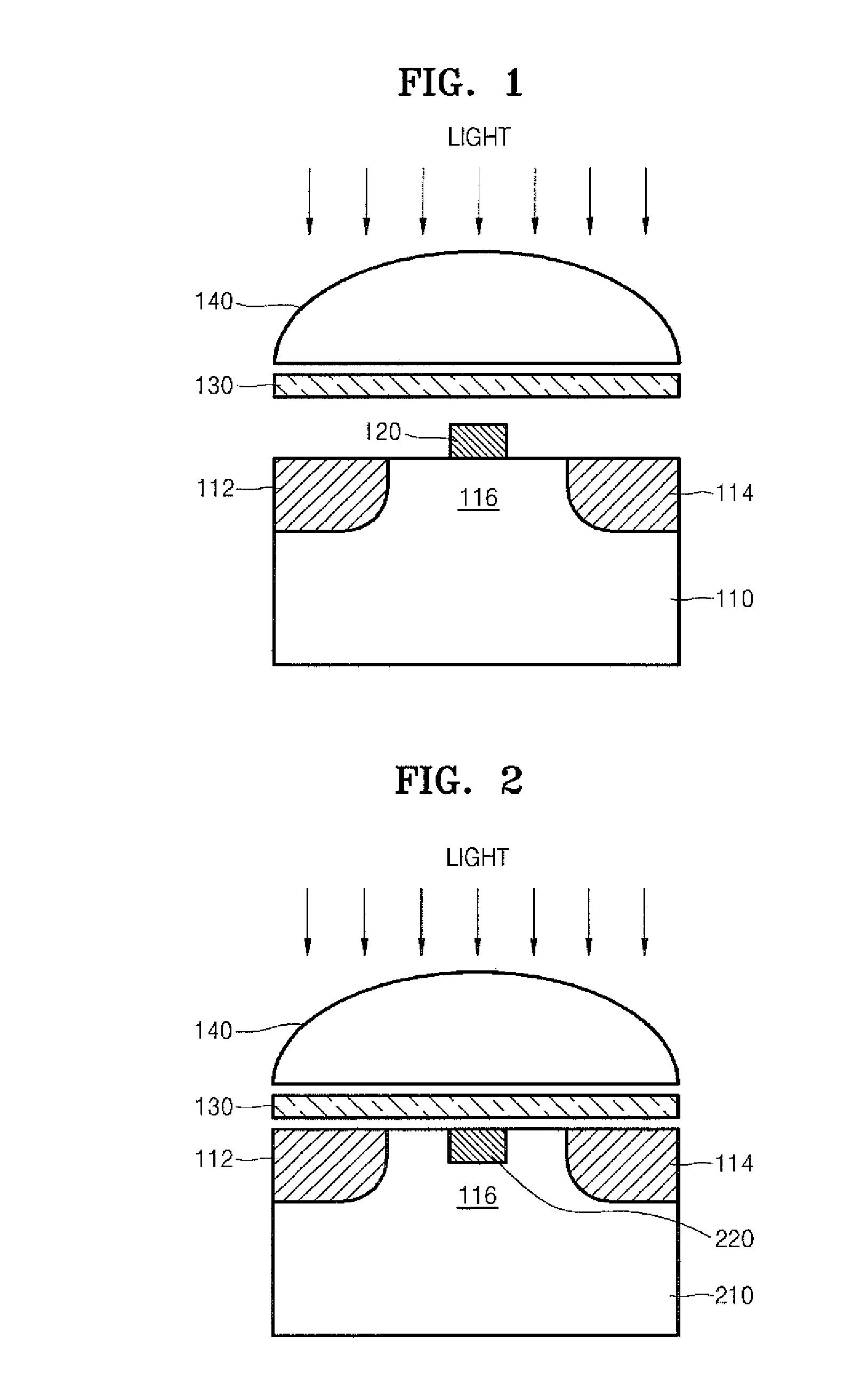
[0037]FIG. 1 is a cross-sectional view of a sub-pixel of an image sensor according to an exemplary embodiment of the present invention.

[0038]Referring to FIG. 1, a f...


PUM


Abstract

An image sensor includes a plurality of pixels disposed in an array, each pixel comprising a first region and a second region, the first region and the second region separated from each other in a semiconductor layer, and doped with impurities having different conductivities from each other, a photoelectric conversion region formed between the first and second regions, and at least one metal nanodot that focuses an incident light onto the photoelectric conversion region.

Description

CROSS-REFERENCE TO RELATED APPLICATION[0001]This application claims priority to Korean Patent Application No. 10-2008-0072438, filed on Jul. 24, 2008, the disclosure of which is incorporated herein in its entirety by reference.BACKGROUND OF THE INVENTION[0002]1. Technical Field[0003]The present disclosure relates to an image sensor, and more particularly to an image sensor having a nanodot.[0004]2. Discussion of the Related Art[0005]A color image sensor is a photoelectric transducer that converts light into an electric signal. A conventional image sensor includes a plurality of unit pixels arranged in an array on a semiconductor substrate. Each unit pixel includes a photodiode and a plurality of transistors. The photodiode generates and stores photocharges by receiving external light, and the transistors output electrical signals according to the generated photocharges.[0006]A complimentary metal oxide semiconductor (CMOS) image sensor includes a photodiode that receives and stores ...

Claims


Application Information

Patent Timeline
IPC IPC(8): H01L31/112H01L31/0232
CPCB82Y20/00H01L27/14643H01L27/14625B82Y30/00H01L27/146
Inventor CHA, DAE-KILJIN, YOUNG-GUMIN, BOK-KIPARK, YOON-DONG
Owner SAMSUNG ELECTRONICS CO LTD
Why Eureka
Try Eureka