Stacked memory module and system

a memory module and stacking technology, applied in the field of memory systems, can solve the problems of reducing the area occupied by the three-dimensional memory device of tanaka, and achieve the effect of increasing the capacity of the memory modul

Active Publication Date: 2010-01-28
SAMSUNG ELECTRONICS CO LTD
View PDF6 Cites 120 Cited by
  • Summary
  • Abstract
  • Description
  • Claims
  • Application Information

AI Technical Summary

Benefits of technology

[0008]In a general aspect of the present invention, a three dimensional memory module / system is formed with a stack of slave and master chips with high memory capacity and efficient wiring and capacity organization for multiple memory banks, bank groups and / or ranks formed in the memory module / system.
[0032]In another aspect of the present invention, a three dimensional memory system includes a first type chip, a plurality of second type chips stacked with the first type chip, and through electrodes formed through at least one of the second type chips. The three dimensional memory system further includes a first signal path disposed on the first type chip and a respective second signal path disposed on each second type chip. In that case, the first signal path is coupled to the respective second signal paths via the through electrodes. In addition, a first length of the first signal path is maximized and a second length of each respective second signal path is minimized.
[0043]In this manner, by forming a master memory core in the master chip for forming the total memory capacity of the memory module with the slave memory cores, the capacity of the memory module is increased. In addition, the memory capacity is organized to have multiple memory banks, bank groups and / or ranks for efficient wiring.

Problems solved by technology

However, Leedy just discloses one three dimensional memory device and not a three dimensional memory module / system.
Such vertical terminals disposed on the outside periphery of the substrates disadvantageously increase the area occupied the three dimensional memory device of Tanaka.

Method used


Image

  • Stacked memory module and system
  • Stacked memory module and system
  • Stacked memory module and system

Examples


Embodiment Construction

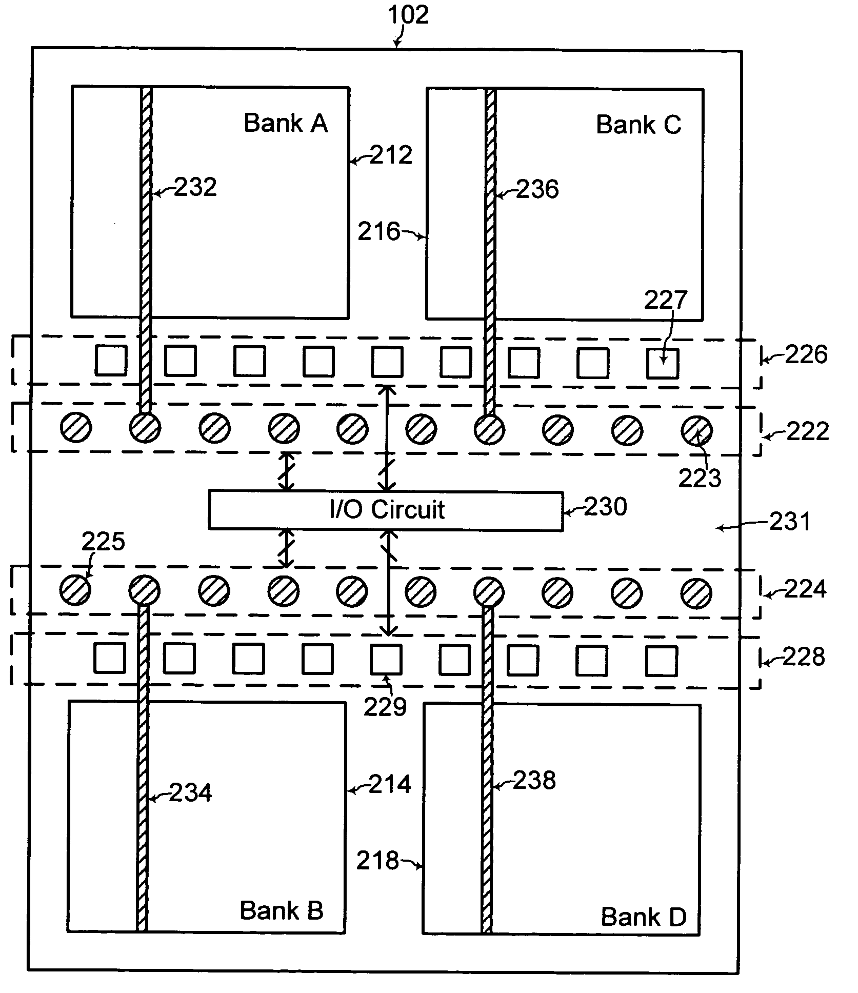
[0075]FIG. 1 shows a cross-sectional view of a three dimensional memory module 100, according to an example embodiment of the present invention. A memory module is broadly defined as an integrated circuit package formed with multiple integrated circuit memory dies (i.e., integrated circuit memory chips) with controlled access to the multiple memory dies. Referring to FIG. 1, the three dimensional memory module 100 includes a master chip 102 mounted on a substrate 104. In addition, a plurality of slave chips 106, 108, and 110 are stacked over the master chip 102.

[0076]A first slave chip 106 is stacked over the master chip 102, a second slave chip 108 is stacked over the first slave chip 106, and a third slave chip 110 is stacked over the second slave chip 108. However, the present invention may be practiced with any number of slave chips stacked over any number of the master chip 102.

[0077]The three dimensional memory module 100 further includes first TSVs (through semiconductor vias...


PUM


Abstract

A three dimensional memory module and system are formed with at least one slave chip stacked over a master chip. Through semiconductor vias (TSVs) are formed through at least one of the master and slave chips. The master chip includes a memory core for increased capacity of the memory module / system. In addition, capacity organizations of the three dimensional memory module / system resulting in efficient wiring is disclosed for forming multiple memory banks, multiple bank groups, and / or multiple ranks of the three dimensional memory module / system.

Description

CROSS-REFERENCE TO RELATED APPLICATION(S) [0001]The present application claims priority under 35 U.S.C. §119 to Korean Patent Application No. 2008-0072904 filed on Jul. 25, 2008 and to Korean Patent Application No. 2008-0125338 filed on Dec. 10, 2008, both of which are incorporated herein by reference in their entirety.TECHNICAL FIELD [0002]The present invention relates generally to memory systems, and more particularly, to a three dimensional stacked memory system with high memory capacity and having efficient wiring and capacity organization for multiple memory banks, bank groups and / or ranks formed in the memory system.BACKGROUND OF THE [0003]The area occupied by an integrated circuit device is desired to be minimized for being used in smaller portable electronic devices. Accordingly, a three dimensional stacked memory device is formed in the prior art for minimizing the area occupied by the memory device.[0004]For example, U.S. Pat. No. 6,133,640 to Leedy discloses a memory devi...

Claims


Application Information

Patent Timeline
Patent Type & Authority Applications(United States)
IPC IPC(8): G11C5/02G11C5/06
CPCG11C5/02G11C5/025G11C5/04G11C8/12H01L2224/16145G11C29/14H01L23/481H01L25/0657H01L2924/15311G11C8/18H01L2224/05026H01L2224/05548H01L2224/05573H01L2224/13025H01L2224/05001H01L2924/00014H01L2224/16237H01L24/05H01L2224/02379H01L2224/05599H01L2224/05099
Inventor KANG, UK-SONGCHUNG, HOE-JUCHOI, JANG-SEOKLEE, HOON
Owner SAMSUNG ELECTRONICS CO LTD
Why Eureka
Try Eureka