Electrooptical high-index contrast waveguide component

a high-index contrast and waveguide technology, applied in the direction of optical waveguide light guide, instruments, etc., can solve the problems of difficult miniaturization of electronic components, waveguide curves often only having large curvature radii, and only very difficult integration of electronic components, etc., to achieve the effect of convenient mass production and easy production

Active Publication Date: 2010-01-28
KARLSRUHER INST FUR TECH
View PDF10 Cites 22 Cited by
  • Summary
  • Abstract
  • Description
  • Claims
  • Application Information

AI Technical Summary

Benefits of technology

[0013]It is a further object of the invention to provide an electro-optical component which is easy to produce and therefore cost-efficient and suitable for mass production.
[0014]It is still a further object of the invention to provide a compact electro-optical component which may be integrated together with electronic components on a common substrate.
[0031]On certain conditions, furthermore, it is advantageous to design the component such that at least 40% of the guided optical power propagates in the low-refractive material.

Problems solved by technology

These modulators have a plurality of disadvantages: On the one hand, they may be integrated only very difficultly in electronic components on a common substrate, since many substrates being usually used to implement electronic components, particularly silicon, have no or only a very poor—and therefore not being technically useable—linear eletro-optical effect.
Furthermore, waveguide curves often may only be provided with large radii of curvature, since the index contrast of the waveguides diffused into is very low.
Therefore, miniaturizing these components is at least difficult.
Furthermore, the mode field diameter is very large due to the low index contrast, and the volume, which has to be filled by the applied electric field, is accordingly large.
The residual electric field unnecessarily increases the stray capacitance being in effect between the electrodes, and therefore the current being necessary for operating the modulator.
In total, these components therefore need high input power, which can mostly be provided by special and expensive driver electronic circuits.
The electric band width of these modulators, however, is comparably poor up to now, since either the life-time of the corresponding charge carriers acts restricting, or the velocity is relevant, with which the necessary amount of charge can be circulated.
Furthermore, producing the small gap between the waveguide stripes and filling it is technologically very demanding.
In case of the components having the same length, this in turn disadvantageously causes a relatively high operating voltage.
Using the waveguide core itself as electrode is also not mentioned, and also not possible with the described metal electrodes, by implication.

Method used


Image

  • Electrooptical high-index contrast waveguide component
  • Electrooptical high-index contrast waveguide component
  • Electrooptical high-index contrast waveguide component

Examples


Embodiment Construction

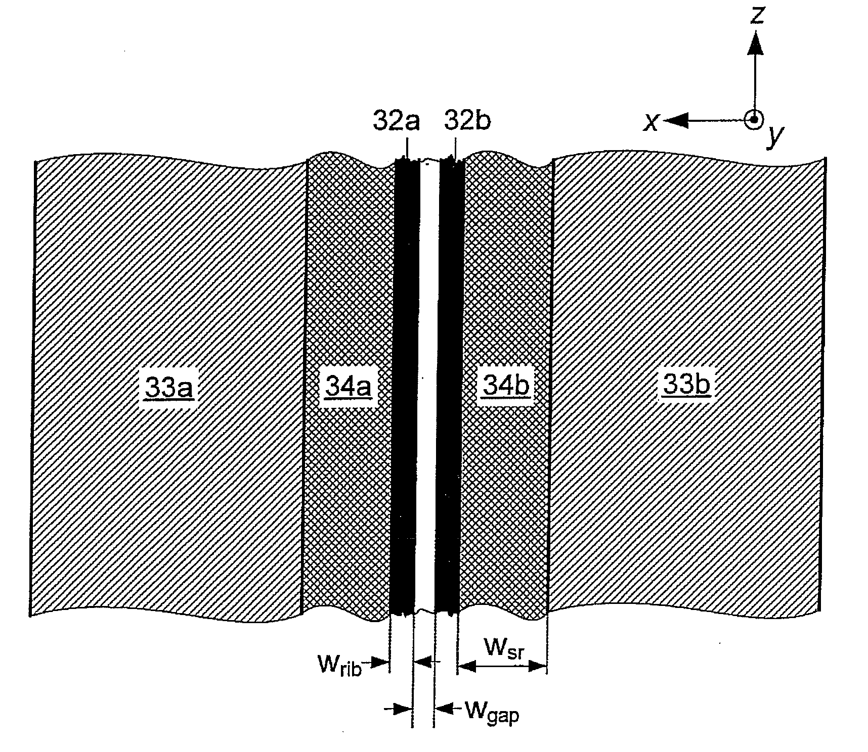
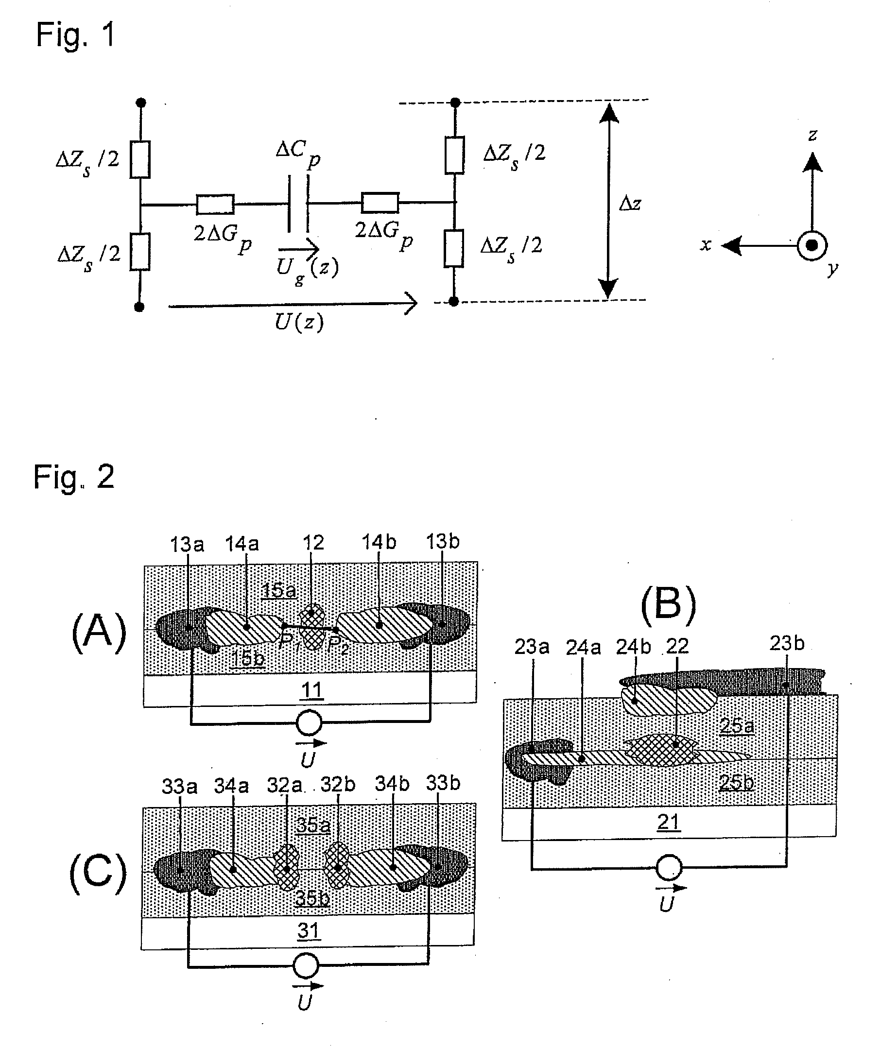
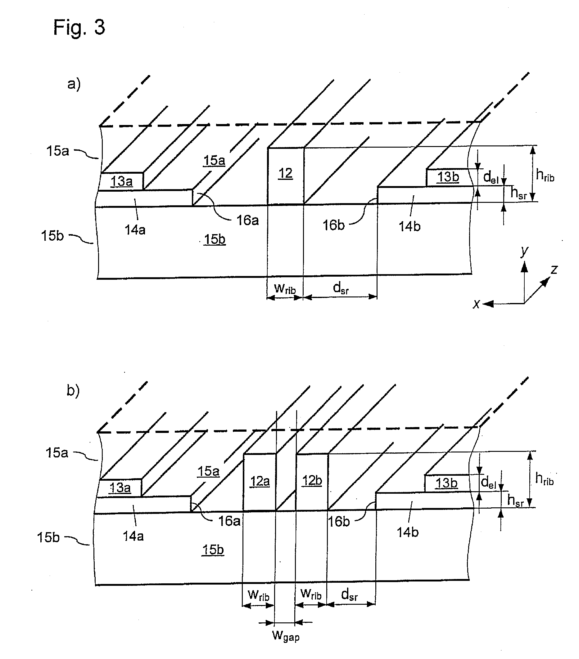
[0052]FIG. 2 shows schematic waveguide cross sections of the three exemplary embodiments of the invention, already addressed. Thereby, the principle arrangement of the different elements is essential. The geometric forms have to be understood as being exemplary. The substrates 11, 21, 31 may consist of one or more layers not being differentiated here, which may serve for implementing electric components, for example.

[0053]The voltage U to be applied for changing the transmission properties is depicted in FIG. 2 in each case. This voltage and / or the current being generated by it allows to change the transmission properties of the waveguide.

[0054]In FIG. 2 (A), the high-refractive one-piece or multi-part waveguide core 12 is surrounded by one or more low-refractive materials 15a, 15b, at least one of these having electro-optical properties. The mode field of the light being guided in the waveguide extends into the electro-optical material. A spatially concentrated electric field havin...


PUM


Abstract

A high-index contrast waveguide component is presented, which is based on the fast changing of the transmission properties of an optical waveguide by applying electric voltages, or by embossing electric currents. The waveguide consists of a high-refractive waveguide core surrounded by a low-refractive surrounding material, which at least area by area has electro-optical properties. By applying a voltage to completely or partially optically transparent electrodes, an electric field is generated having a strong overlap with the optical mode, being in interaction with it, and therefore changing the transmission properties of the waveguide. The transparent electrodes or supply line areas are laminar, connected at low resistance with conductor paths of high conductivity by means of structures continually repeated along the propagation direction. Thus, it is possible for example to very fast load the capacity being effective between the electrodes, and to thus achieve a high electric band width. In certain embodiments, the waveguide core itself consists of one or more electrically conductive stripes being used as electrodes at the same time. These embodiments make especially small switching voltages possible.For example, the presented component makes fast electro-optical modulators with small switching voltages possible, which modulators may be integrated together with electronic components on a common semiconductor substrate (e.g. silicon).

Description

FIELD OF THE INVENTION[0001]The invention relates to an electro-optical high-index contrast waveguide component, particularly for integrated optics and optical telecommunication engineering.BACKGROUND OF THE INVENTION[0002]Using light for information transfer offers a series of advantages in comparison to pure electrical procedures, primarily, when high data rates are needed or long distances have to be covered. In contrast, digital processing and storage of information is today carried out almost exclusively electronically in integrated components, which are mostly produced on the basis of silicon, for in example in Complementary Metal Oxide Semiconductor Technology (CMOS). For converting information between electronic storage and processing components and optical transmission lines, electro-optical components, which may be integrated with electronic circuits, therefore are of great interest.[0003]Today, fast electro-optical modulators are mostly integrated on substrates, which hav...

Claims


Application Information

Patent Timeline
Patent Type & Authority Applications(United States)
IPC IPC(8): G02B6/00
CPCG02F1/011G02F1/025G02F2202/104G02F1/065G02F2201/127G02F1/0316
Inventor KOOS, CHRISTIANLEUTHOLD, JURGFREUDE, WOLFGANGBROSI, JAN MICHAEL
Owner KARLSRUHER INST FUR TECH
Why Eureka
Try Eureka