Semiconductor device and method of designing the same

a technology of semiconductor devices and solder balls, applied in the direction of semiconductor devices, semiconductor/solid-state device details, instruments, etc., can solve the problems of limited degree of freedom in design, large cost, and deformation of semiconductor packages, and achieve the effect of simple method

Inactive Publication Date: 2010-02-04
RENESAS ELECTRONICS CORP
View PDF6 Cites 10 Cited by
  • Summary
  • Abstract
  • Description
  • Claims
  • Application Information

AI Technical Summary

Benefits of technology

[0012]According to the present invention, unbalanced stress possibly exerted to an int

Problems solved by technology

However, there has been known a problem of deformation of semiconductor packages due to unbalanced stress exerted by the semiconductor chip(s) to the interposer, for the case where the semiconductor chip(s) have a rectangular geometry in a plan view, or for the case where the center of the interposer does not coincide with the center of the semiconductor chip(s).
This sort of deformation may cause warping or

Method used


Image

  • Semiconductor device and method of designing the same
  • Semiconductor device and method of designing the same
  • Semiconductor device and method of designing the same

Examples


first embodiment

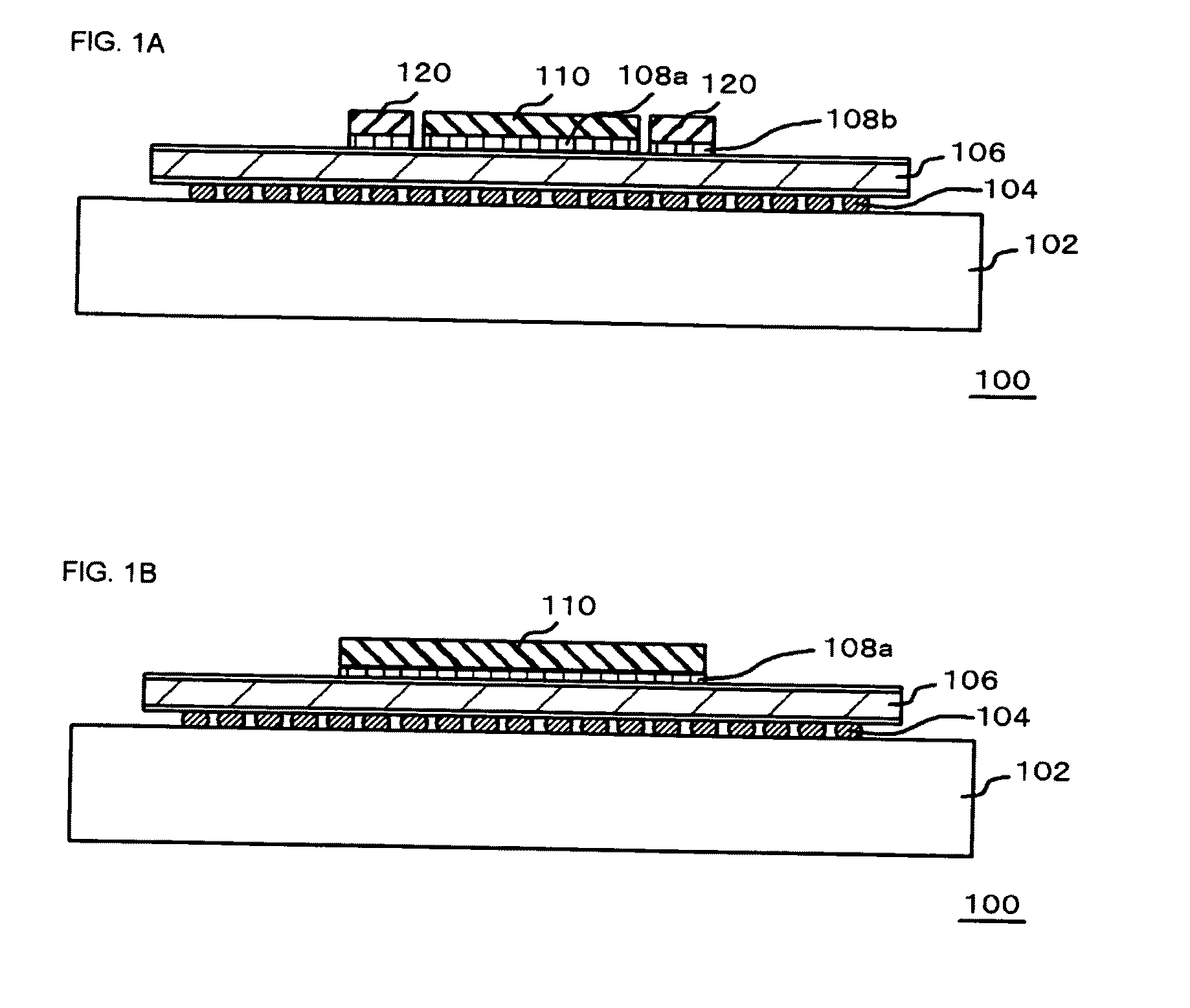
[0035]FIGS. 1A and 1B are sectional views illustrating a configuration of a semiconductor device of this embodiment.

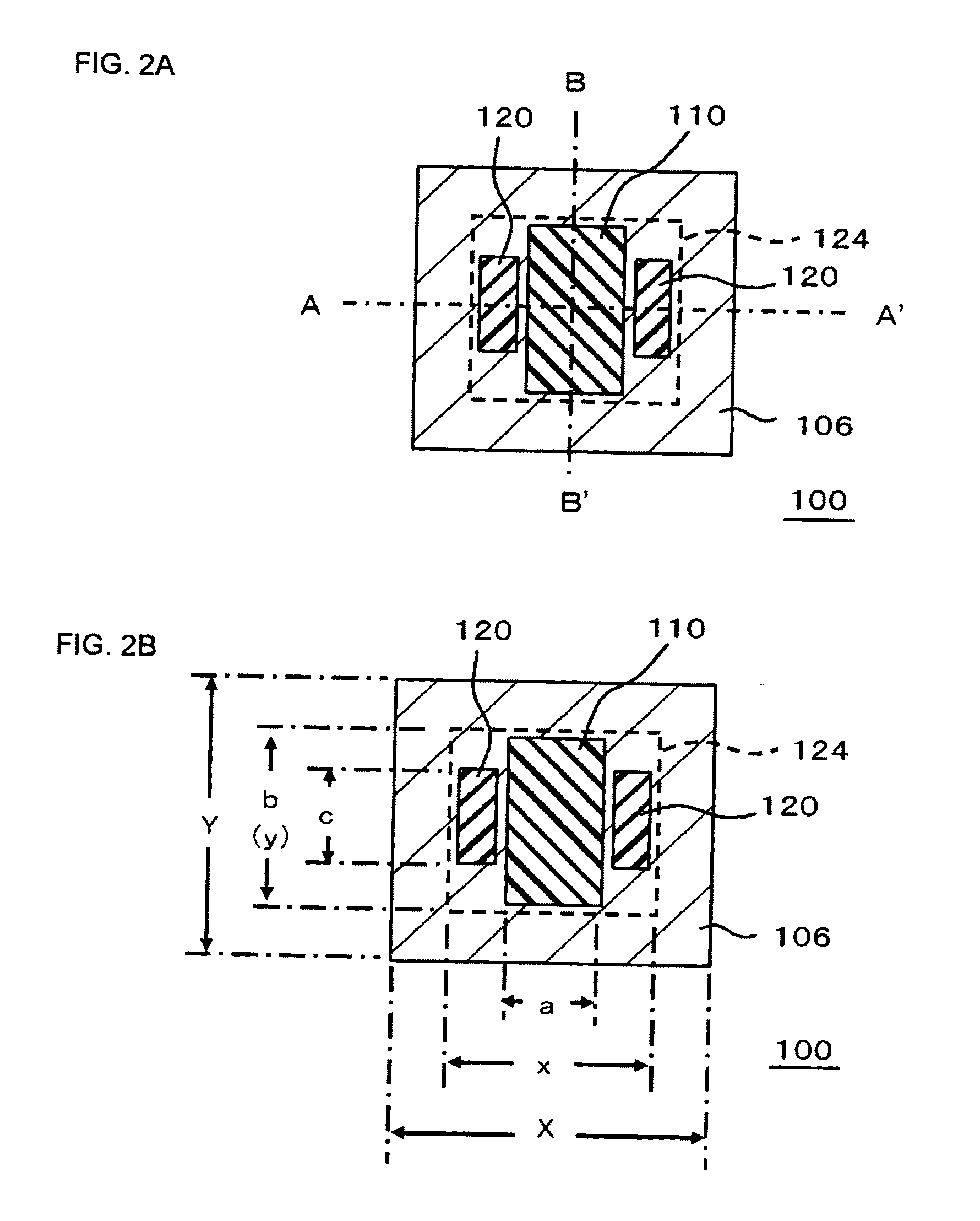
[0036]FIGS. 2A and 2B are plan views of the semiconductor device 100. FIG. 1A corresponds to a sectional view taken along line A-A′ in FIG. 2A, and FIG. 1B corresponds to a sectional view taken along line B-B′ in FIG. 2A. Dimensions of the individual components of a semiconductor device are given in FIG. 2B.

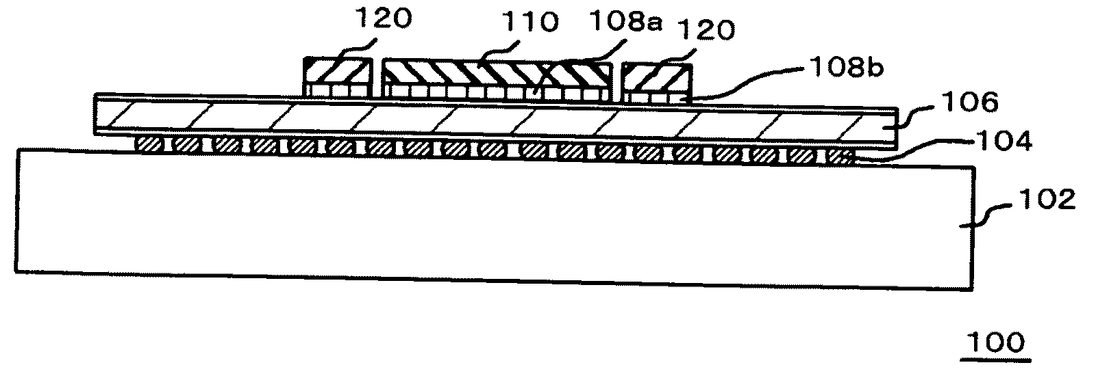
[0037]The semiconductor device 100 contains a mounting substrate 102, an interposer 106 mounted over the mounting substrate 102 while placing solder balls 104 in between, and a semiconductor chip 110 disposed over the interposer (wiring board) 106. In this embodiment, the semiconductor device 100 may be a semiconductor package configured to have the interposer 106 mounted by surface mounting using the solder balls 104 onto the mounting substrate 102 such as FCBGA (Flip Chip Ball Grid Array), PBGA (Plastic Ball Grid Array), and FPBGA (Fine Pitched Ball Grid Array).

[0...

second embodiment

[0063]FIGS. 6A and 6B are plan views illustrating a configuration of the semiconductor device 100 in this embodiment. FIG. 6A illustrates dimensions of the individual constituents of the semiconductor device 100. FIG. 6B illustrates the center 106c of the interposer 106. In this embodiment, the dimension of the semiconductor chip 110 and the location thereof over the interposer 106 are different from those in the first embodiment.

[0064]In this embodiment, the semiconductor chip 110 has a geometry analogous to that of the interposer 106 in a plan view, while aligning the longitudinal direction thereof in the same direction. In other words, the relation X:Y=a:b is satisfied. On the other hand, the center of the semiconductor chip 110 in this embodiment does not coincide with the center 106c of the interposer 106. In this configuration, disposition of only of the semiconductor chip 110 over the interposer 106 may result in unbalanced stress exerted by the semiconductor chip 110 to the ...

third embodiment

[0072]FIGS. 9A and 9B are plan views illustrating a configuration of the semiconductor device 100 of this embodiment. In this embodiment, the semiconductor device 100 further includes a semiconductor chip 112, in addition to the semiconductor chip 110 explained in the first embodiment and so forth. In this embodiment, the semiconductor device 100 may be given as a SiP (system in package) having a plurality of semiconductor chip mounted therein.

[0073]The semiconductor chip 110 and the semiconductor chip 112 are disposed side by side. In this embodiment, as illustrated in FIG. 9B, the first outer circumferential region 126 may be given as an area which surrounds the semiconductor chip 110 and the semiconductor chip 112 disposed over the interposer 106. The first outer circumferential region 126 has length “a” in the transverse direction of the drawing, and has length “b” in the longitudinal direction. The first outer circumferential region 126 herein does not have a shape analogous to...


PUM


Abstract

A semiconductor device contains an interposer having a square planar geometry, with length X for a first edge and length Y for a second edge orthogonal to the first edge, and a semiconductor chip and a dummy component disposed over the interposer, wherein the center of a first outer circumferential region, which surrounds the semiconductor chip over the interposer, and has length “a” for a third edge, and length “b” for a fourth edge, does not coincide with the center of the interposer, or equation X:Y=a:b is not satisfied, and the center of a second outer circumferential region, which surrounds the first outer circumferential region and the dummy components disposed over the interposer, and has length “x” for a fifth edge, and length “y” for a sixth edge, coincides with the center of the interposer, and equation X:Y=x:y is satisfied.

Description

[0001]This application is based on Japanese patent application No. 2008-194914 the content of which is incorporated hereinto by reference.BACKGROUND[0002]1. Technical Field[0003]The present invention relates to a semiconductor device and a method of designing the same, and in particular to a semiconductor device having an interposer and a semiconductor chip disposed thereon, and a method of designing the same.[0004]2. Related Art[0005]Semiconductor packages are generally configured by mounting an interposer on a mounting substrate while placing solder balls in between, and by disposing semiconductor chip(s) further thereon. However, there has been known a problem of deformation of semiconductor packages due to unbalanced stress exerted by the semiconductor chip(s) to the interposer, for the case where the semiconductor chip(s) have a rectangular geometry in a plan view, or for the case where the center of the interposer does not coincide with the center of the semiconductor chip(s)....

Claims


Application Information

Patent Timeline
IPC IPC(8): H01L23/488G06F17/50
CPCH01L23/562H01L25/0655H01L2924/19105H01L2924/3511H01L2924/15311H01L2224/48227H01L2224/16225H01L2224/73265H01L2224/73204H01L2224/32225H01L2924/00012H01L2924/00H01L24/73H01L2924/00014H01L2924/00011H01L2224/0401
Inventor KAKEGAWA, CHIKA
Owner RENESAS ELECTRONICS CORP
Why Eureka
Try Eureka