Determining on chip loading impedance of RF circuit

a technology of rf circuit and impedance, applied in the field of devices and circuits, can solve the problems of only limited by losses, large voltage swings across load, and dissipation of dc current, and achieve the effect of improving or monitoring the performance of the amplifier or of downstream circuits such as filters

Active Publication Date: 2010-02-04
NXP BV
View PDF8 Cites 23 Cited by
  • Summary
  • Abstract
  • Description
  • Claims
  • Application Information

AI Technical Summary

Benefits of technology

[0011]By determining the matched output impedance, the performance of the amplifier or of downstream circuits such as filters, can be improved or monitored. The amplifier output can be detected directly at the output of the amplifier, or downstream after a matching network or further downstream.

Problems solved by technology

However this arrangement dissipates DC current.
But having a too high load, will cause large voltage swings across the load, and at a certain point, the output transistor (current source) will saturate and clip.
This will cause distortion.
The source impedance comes from the transmitter, with is typically an open collector structure, and thus is high impedance, only limited by losses.
Thus the SAW performance is degraded, showing for example an in-band ripple, and worse suppression of out-of-band signal components.
It is nevertheless difficult to determine what value the resistance should have as it is hard to measure the impedance effects of external matching tracks, external components, the package and of the bond-wires and so on, on RF signals.

Method used


Image

  • Determining on chip loading impedance of RF circuit
  • Determining on chip loading impedance of RF circuit
  • Determining on chip loading impedance of RF circuit

Examples


Embodiment Construction

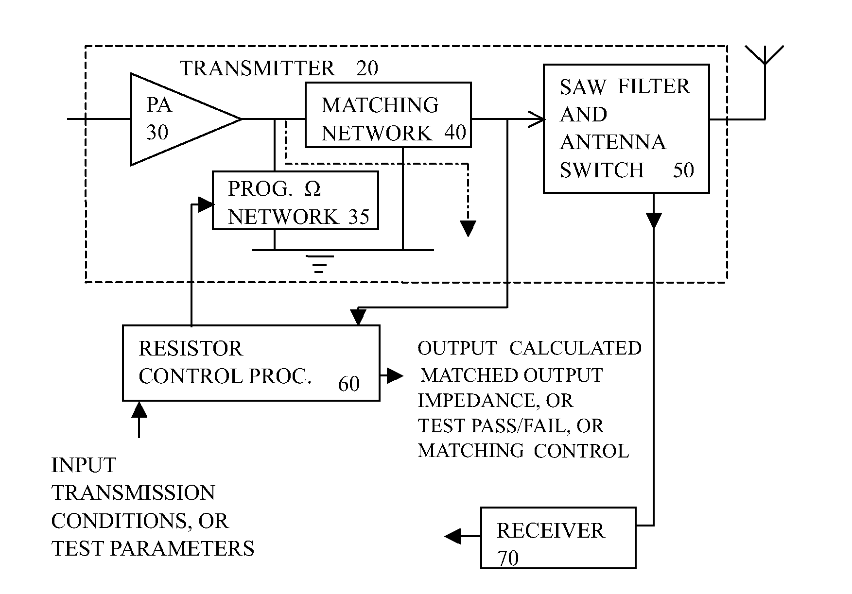
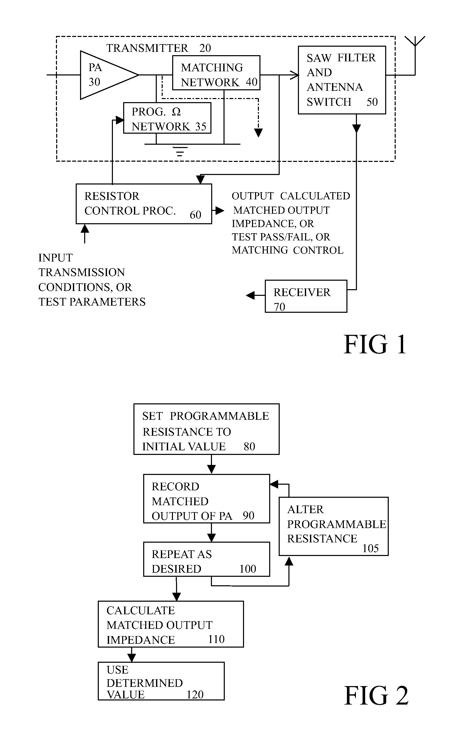
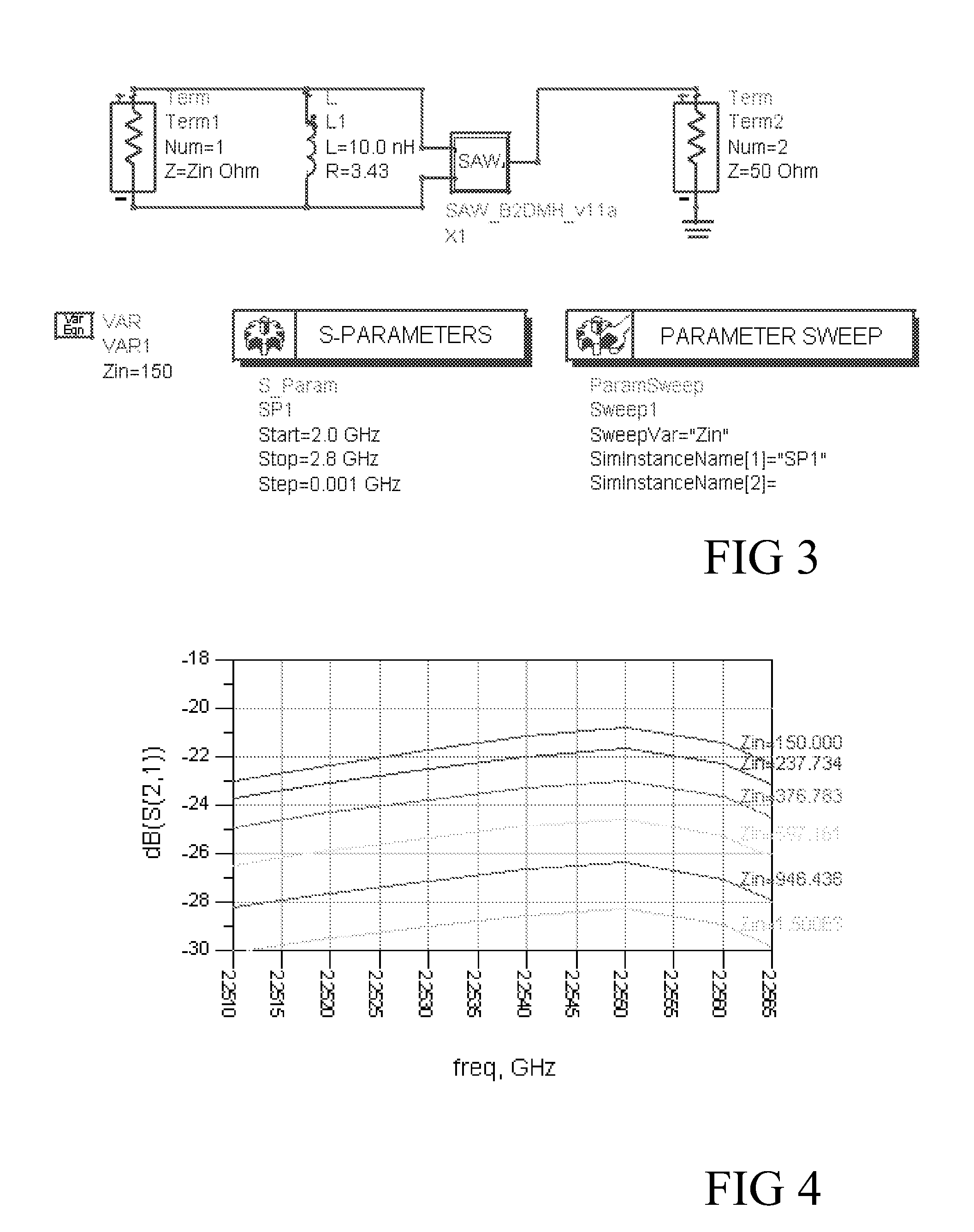
[0025]The present invention will be described with respect to particular embodiments and with reference to certain drawings but the invention is not limited thereto but only by the claims. The drawings described are only schematic and are non-limiting. In the drawings, the size of some of the elements may be exaggerated and not drawn on scale for illustrative purposes. Where the term “comprising” is used in the present description and claims, it does not exclude other elements or steps. Where an indefinite or definite article is used when referring to a singular noun e.g. “a” or “an”, “the”, this includes a plural of that noun unless something else is specifically stated.

[0026]The term “comprising”, used in the claims, should not be interpreted as being restricted to the means listed thereafter; it does not exclude other elements or steps. Thus, the scope of the expression “a device comprising means A and B” should not be limited to devices consisting only of components A and B. It ...


PUM


Abstract

An R.F. transmitter circuit has an amplifier (30), a matching network (40) coupled to an output of the amplifier, a programmable resistance (35) coupled to the output of the amplifier, and a controller (60) arranged to control the programmable resistance, and to determine a matched output impedance of the amplifier by detecting a change in the amplifier output for different values of the programmable resistance. This output impedance can be used to adjust the matching to achieve optimum gain or optimum efficiency or other characteristic, during manufacture, test, or in use.

Description

FIELD OF THE INVENTION[0001]This invention relates to device and circuits such as integrated semiconductor devices arranged to determine a load impedance of a circuit, e.g. an on-chip load impedance and to corresponding methods.DESCRIPTION OF THE RELATED ART[0002]It is known to provide on-chip termination for driver circuits for high speed data transmission applications by adding a matching resistor in parallel with the load on the output of the driver. US patent application 20030116810 explains that it would be desirable to provide an adjustable resistance using an off-chip device having selectable resistance, which can be selected by a digital signal periodically updated according to changes in conditions such as voltage and temperature. This document proposes a programmable impedance control circuit for use with an external resistor and having a voltage divider coupled to the external resistor and other components to generate various impedance values.[0003]U.S. Pat. No. 6,429,685...

Claims


Application Information

Patent Timeline
Patent Type & Authority Applications(United States)
IPC IPC(8): H04B17/00
CPCH03F1/0205H03F1/32H03F1/56H03F3/191H03H7/40H03F2200/378H03F2200/387H03F2200/391H03F3/24
Inventor VISSER, HENDRIK A.
Owner NXP BV
Why Eureka
Try Eureka