Nonvolatile memory device and method of manufacturing the same

a memory device and non-volatile technology, applied in the direction of digital storage, semiconductor/solid-state device details, instruments, etc., can solve the problems of diode itself being thermally broken down, information rewriting is difficult, and the off current required for appropriate reading cannot be maintained

Active Publication Date: 2010-02-11
HITACHI LTD
View PDF6 Cites 74 Cited by
  • Summary
  • Abstract
  • Description
  • Claims
  • Application Information

AI Technical Summary

Benefits of technology

[0009]It is an object of the present invention to provide a technique capable of realizing a memory cell structure in which a diode is less likely to become a high temperature even when the phase-change material is set at a high temperature in a nonvolatile memory device comprising a phase-change memory configured by cross-point memory cells in which a memory element formed of a phase-change material and a selection element formed of a diode are combined.
[0020]It is possible to realize a memory cell structure in which a diode is less likely to be at a high temperature even when a phase-change material is set at a high temperature.

Problems solved by technology

However, when the diode is at a high temperature, an impurity profile inside the diode breaks, which causes a problem that the OFF current required for appropriate reading can not be maintained or the diode itself is thermally broken down.
It is also possible to use a material having a high thermal conductivity for a material of the diode not to make the diode to be a high temperature, but in this case, there will be caused a problem that a high current is required to set the phase-change material at a high temperature or the required high temperature is not reached to make information rewriting difficult.

Method used


Image

  • Nonvolatile memory device and method of manufacturing the same
  • Nonvolatile memory device and method of manufacturing the same
  • Nonvolatile memory device and method of manufacturing the same

Examples


first embodiment

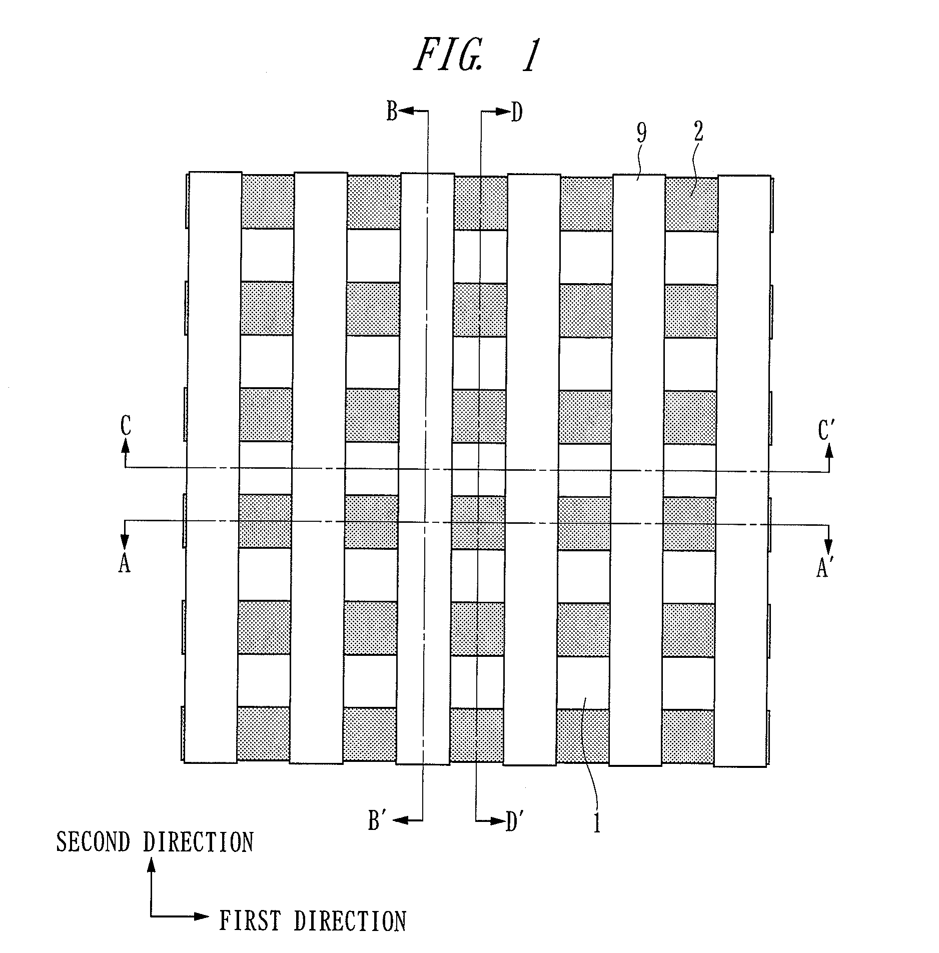
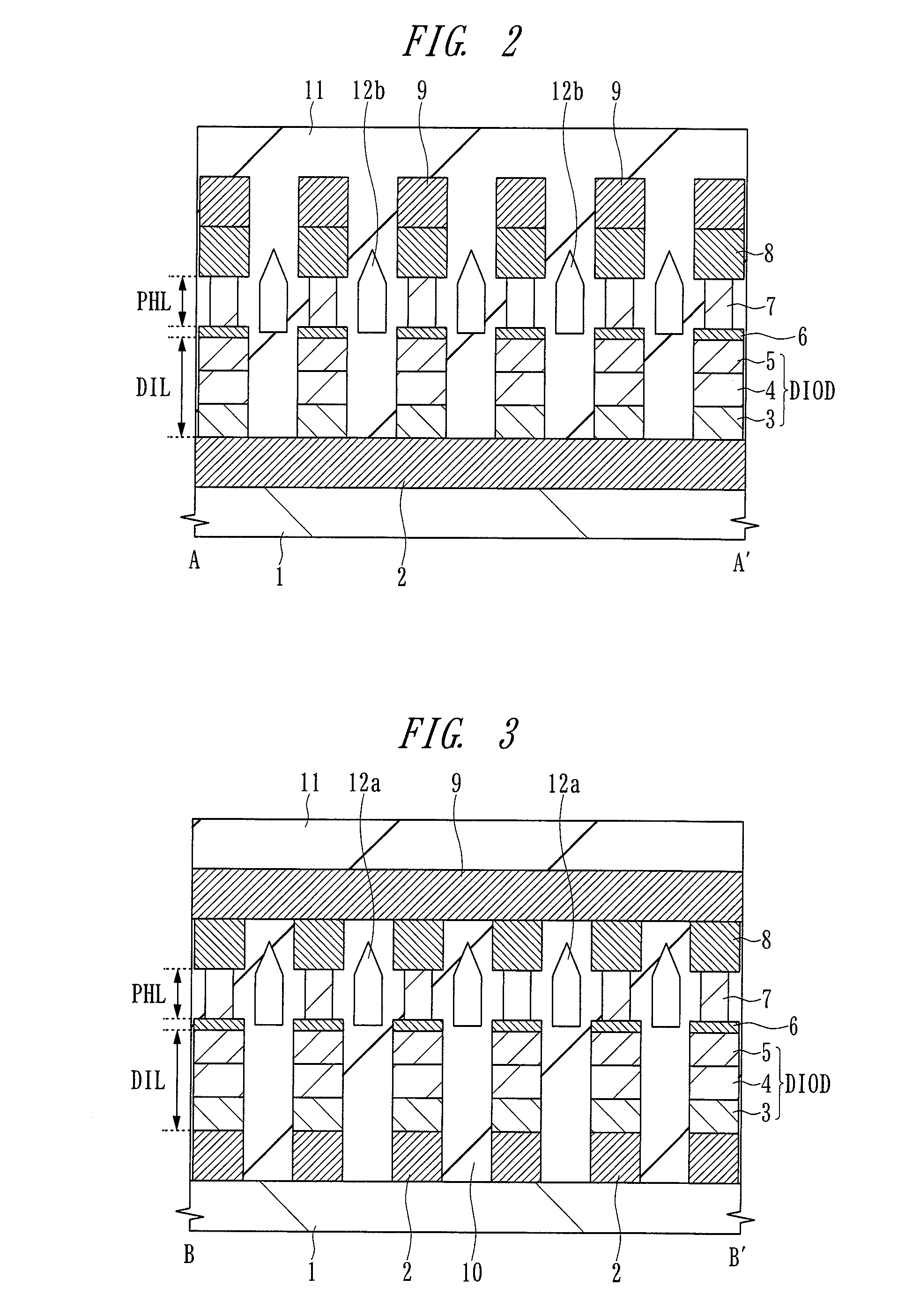
[0085]A memory matrix of a phase-change memory according to a first embodiment will be described with reference to FIG. 1 to FIG. 5. FIG. 1 is a top view of the memory matrix, FIG. 2 is a cross-sectional view of main parts of the memory matrix taken along the line A-A′ of FIG. 1, FIG. 3 is a cross-sectional view of main parts of the memory matrix taken along the line B-B′ of FIG. 1, FIG. 4 is a cross-sectional view of main parts of the memory matrix taken along the line C-C′ of FIG. 1, and FIG. 5 is a cross-sectional view of main parts of the memory matrix taken along the line D-D′ of FIG. 1. In FIG. 1, only a third metal wiring, a first metal wiring and a semiconductor substrate are illustrated for facilitating understanding of the structure of the memory matrix.

[0086]In the figures, reference numeral 1 denotes a semiconductor substrate and reference numeral 2 denotes a first metal wiring extending along a first direction. Further, reference numeral 3 denotes a first polycrystallin...

second embodiment

[0118]A memory matrix of a phase-change memory according to a second embodiment will be described with reference to FIGS. 23 to 25. FIG. 23 is a top view of the memory matrix, FIG. 24 is a cross-sectional view of main parts of the memory matrix taken along the line A-A′ of FIG. 23, and FIG. 25 is a cross-sectional view of main parts of the memory matrix taken along the line B-B′ of FIG. 23. In FIG. 23, only a third metal wiring 9, a first metal wiring 2, and a semiconductor substrate 1 are illustrated for facilitating understanding of the structure of the memory matrix. In the figures, similarly as in the first embodiment described above, reference numeral 1 denotes a semiconductor substrate and reference numeral 2 denotes a first metal wiring extending along a first direction. Further, reference numeral 3 denotes a first polycrystalline silicon film, reference numeral 4 denotes a second polycrystalline silicon film, reference numeral 5 denotes a third polycrystalline silicon film, ...

third embodiment

[0137]A memory matrix of a phase-change memory according to a third embodiment will be described with reference to FIGS. 38 to 40. FIG. 38 is a top view of the memory matrix, FIG. 39 is a cross-sectional view of main parts of the memory matrix taken along the line A-A′ of FIG. 38, and FIG. 40 is a cross-sectional view of main parts of the memory matrix taken along the line B-B′ of FIG. 38. In FIG. 38, only a third metal wiring, a first metal wiring, and a semiconductor substrate are illustrated for facilitating understanding of a structure of the memory matrix. In the figures, similarly as those in the first embodiment described above, reference numeral 1 denotes a semiconductor substrate and reference numeral 2 denotes a first metal wiring extending along a first direction. Further, reference numeral 3 denotes a first polycrystalline silicon film, reference numeral 4 denotes a second polycrystalline silicon film, reference numeral 5 denotes a third polycrystalline silicon film, and...


PUM


Abstract

Provided is a nonvolatile memory device including a phase-change memory configured with cross-point memory cells in which memory elements formed of a phase-change material and selection elements formed with a diode are combined. A memory cell is configured with a memory element formed of a phase-change material and a selection element formed with a diode having a stacked structure of a first polycrystalline silicon film, a second polycrystalline silicon film, and a third polycrystalline silicon film. The memory cells are arranged at intersection points of a plurality of first metal wirings extending along a first direction with a plurality of third metal wirings extending along a second direction orthogonal to the first direction. An interlayer film is formed between adjacent selection elements and between adjacent memory elements, and voids are formed in the interlayer film provided between the adjacent memory elements.

Description

CROSS-REFERENCE TO RELATED APPLICATION[0001]The present application claims priority from Japanese Patent Application No. JP 2008-202771 filed on Aug. 6, 2008, the content of which is hereby incorporated by reference into this application.TECHNICAL FIELD OF THE INVENTION[0002]The present invention relates to a nonvolatile memory device and a method of manufacturing the same. More particularly, the present invention relates to a technique effectively applied to a nonvolatile memory device comprising a phase-change memory that stores a resistance value determined by a phase change between a crystalline state and an amorphous state of a metal compound in a nonvolatile manner and is electrically rewritable, and a manufacture of the nonvolatile memory device.BACKGROUND OF THE INVENTION[0003]Some nonvolatile storage / memory devices utilize a crystalline state and an amorphous state of a metal compound as storage / memory information and a tellurium compound is typically used as its storage / me...

Claims


Application Information

Patent Timeline
Patent Type & Authority Applications(United States)
IPC IPC(8): H01L45/00
CPCG11C11/5678G11C13/0004G11C2213/72H01L27/2409H01L27/2481Y10S438/90H01L45/1233H01L45/1293H01L45/144H01L45/1675H01L45/06H10B63/20H10B63/80H10B63/84H10N70/231H10N70/826H10N70/8616H10N70/8828H10N70/063H10N70/8825
Inventor KINOSHITA, MASAHARUSASAGO, YOSHITAKATAKAURA, NORIKATSU
Owner HITACHI LTD
Why Eureka
Try Eureka