Integrated Circuit Structure, Design Structure, and Method Having Improved Isolation and Harmonics

a technology of integrated circuits and design structures, applied in the direction of transistors, radio frequency switches, instruments, etc., can solve the problems of integrated circuit devices formed in or above the active semiconductor layer, integrated circuit devices such as radio frequency switches, suffer further, and semiconductor-on-insulator wafers suffer performance degradation, etc., to improve isolation, improve isolation, and reduce harmonics

Active Publication Date: 2010-02-11
GLOBALFOUNDRIES US INC
View PDF22 Cites 27 Cited by
  • Summary
  • Abstract
  • Description
  • Claims
  • Application Information

AI Technical Summary

Benefits of technology

[0004]In view of the foregoing disclosed herein are embodiments of a semiconductor structure, a design structure for the semiconductor structure and a method of forming the semiconductor structure. The embodiments reduce harmonics and improve isolation between the active semiconductor layer and the substrate of a semiconductor-on-insulator (SOI) wafer. Specifically, the embodiments incorporate a deep trench isolation region extending to a fully or partially amorphized region of the SOI wafer substrate located either at the top surface of the substrate or embedded withi

Problems solved by technology

Integrated circuit devices formed in or above the active semiconductor layer (e.g., the active silicon layer) of a semiconductor-on-insulator (SOI) wafer often suffer from performance degradation due to coupling capacitance between the integrated circuit devices and the wafer substrat

Method used


Image

  • Integrated Circuit Structure, Design Structure, and Method Having Improved Isolation and Harmonics
  • Integrated Circuit Structure, Design Structure, and Method Having Improved Isolation and Harmonics
  • Integrated Circuit Structure, Design Structure, and Method Having Improved Isolation and Harmonics

Examples


Embodiment Construction

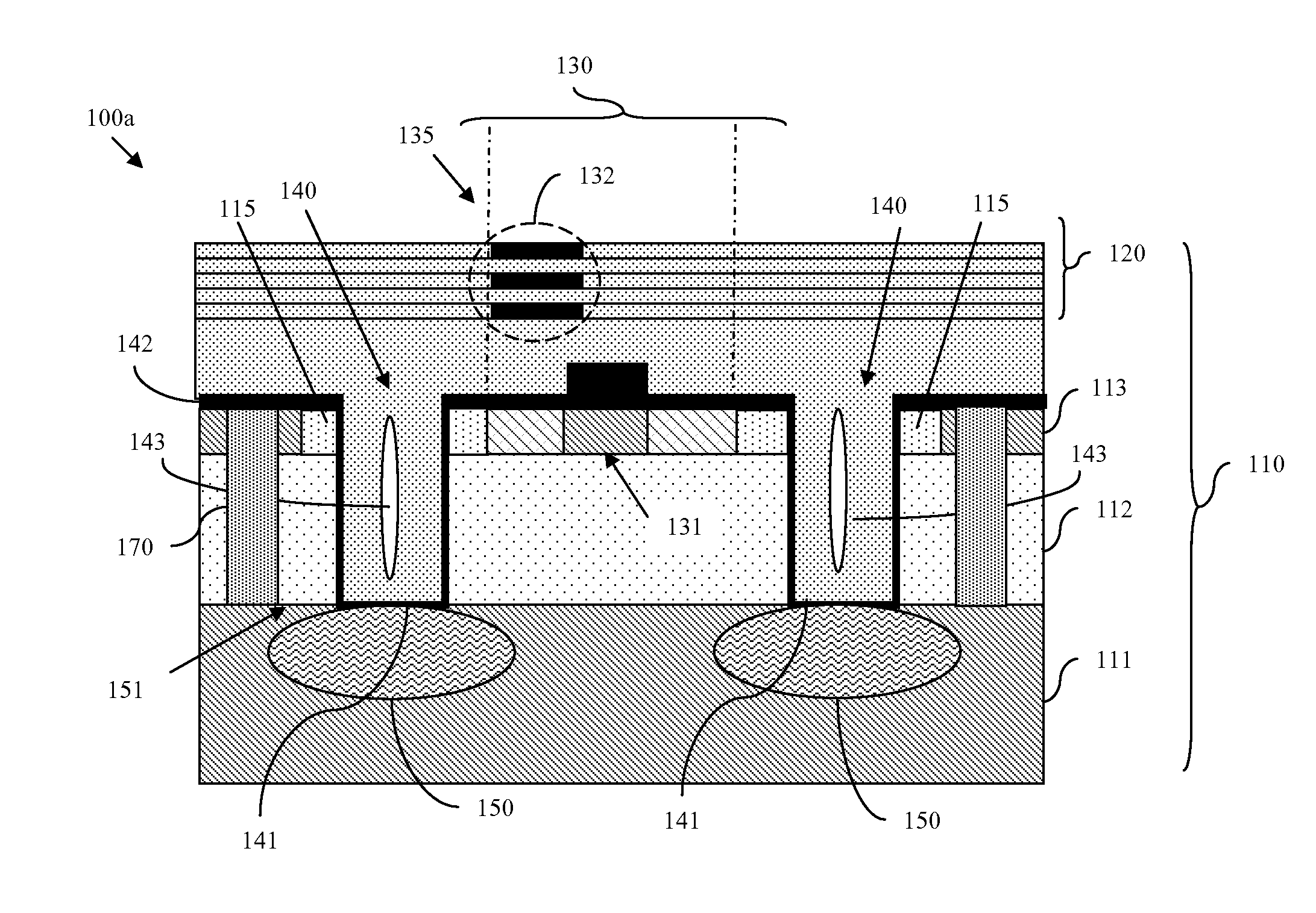
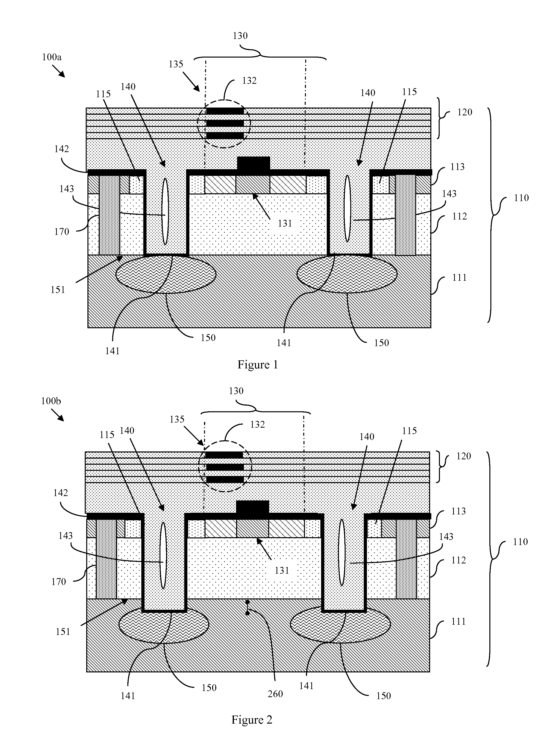
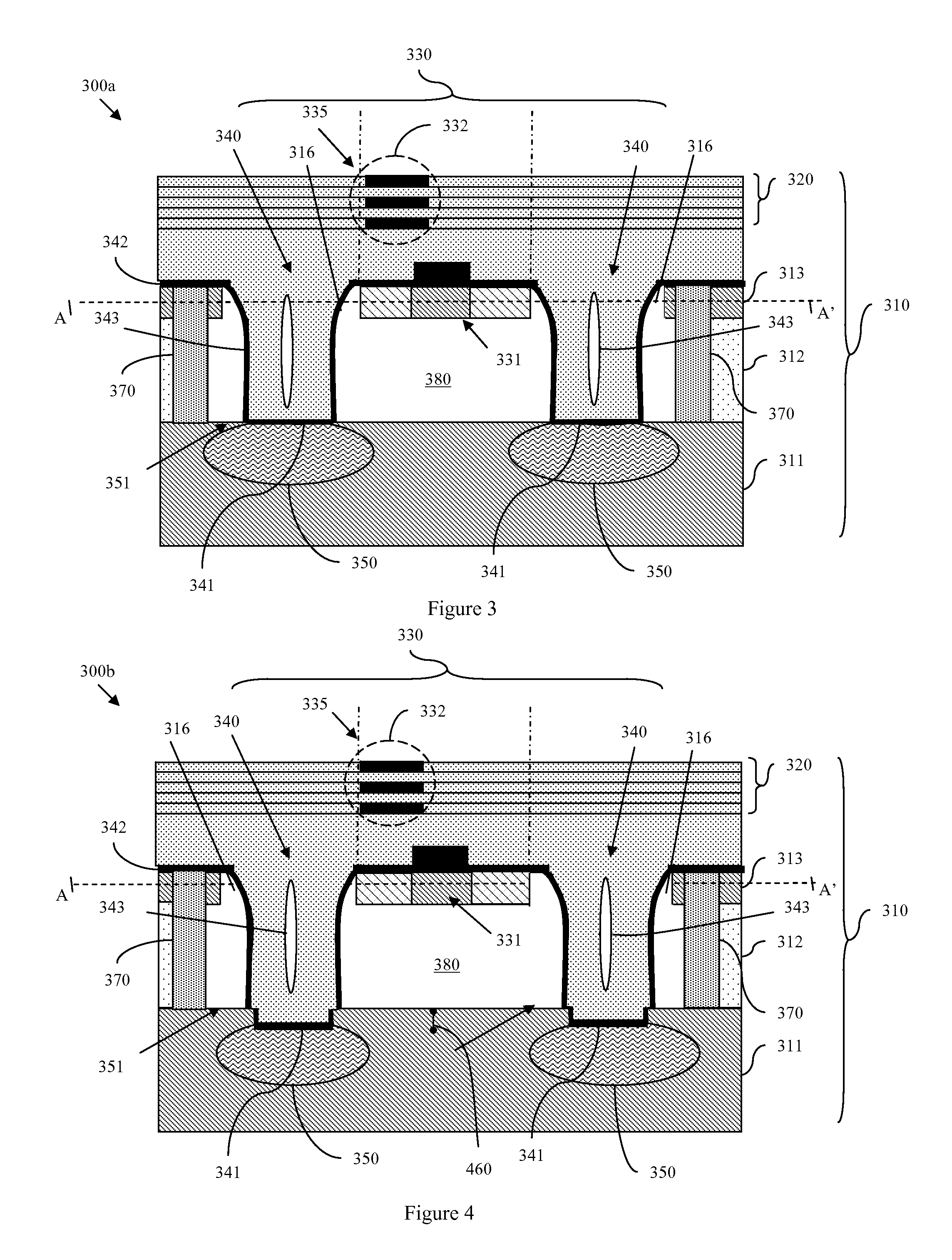
[0035]The embodiments of the invention and the various features and advantageous details thereof are explained more fully with reference to the non-limiting embodiments that are illustrated in the accompanying drawings and detailed in the following description.

[0036]As mentioned above, integrated circuit devices formed in or above the active semiconductor layer (e.g., the active silicon layer) of a semiconductor-on-insulator (SOI) wafer often suffer from performance degradation due to coupling capacitance between the integrated circuit devices and the wafer substrate (e.g., a silicon substrate). Some integrated circuit devices, such as radio frequency (RF) switches, further suffer due to harmonics resulting from the resulting charge layer at the interface between the SOI insulator layer (e.g., the buried oxide (BOX) layer) and the wafer substrate. Therefore, there is a need in the art for a semiconductor structure that is formed using an SOI wafer and that has reduced harmonics and ...


PUM


Abstract

Disclosed are embodiments of a semiconductor structure, a design structure for the semiconductor structure and a method of forming the semiconductor structure. The embodiments reduce harmonics and improve isolation between the active semiconductor layer and the substrate of a semiconductor-on-insulator (SOI) wafer. Specifically, the embodiments incorporate a trench isolation region extending to a fully or partially amorphized region of the wafer substrate. The trench isolation region is positioned outside lateral boundaries of at least one integrated circuit device located at or above the active semiconductor layer of the SOI wafer and, thereby improves isolation. The fully or partially amorphized region of the substrate reduces substrate mobility, which reduces the charge layer at the substrate/BOX interface and, thereby reduces harmonics. Optionally, the embodiments can incorporate an air gap between the wafer substrate and integrated circuit device(s) in order to further improve isolation.

Description

CROSS-REFERENCE TO RELATED APPLICATIONS[0001]This application is related to the following co-pending application filed concurrently herewith by the same Applicants and assigned to the same Assignee, namely, International Business Machines Corporation (IBM Corporation): “INTEGRATED CIRCUIT STRUCTURE, DESIGN STRUCTURE, AND METHOD HAVING IMPROVED ISOLATION AND HARMONICS”, Attorney Docket No. BUR920080080US1. The complete disclosure of this related co-pending application is incorporated herein by reference.BACKGROUND OF THE INVENTION[0002]The embodiments of the invention generally relate to integrated circuit structures and, more specifically, to an integrated circuit structure, a design structure for the integrated circuit structure and a method of forming the integrated circuit structure with improved isolation and, in the case of a radio frequency (RF) device (e.g., a RF switch) with reduced harmonics.[0003]Integrated circuit devices formed in or above the active semiconductor layer ...

Claims


Application Information

Patent Timeline
IPC IPC(8): H01L23/58G06F17/50
CPCH01L21/76289H01L21/764H01L23/585H01L23/66H01L2924/0002H01L27/12H01L2924/00
Inventor BROWN, BRENNAN J.ELLIOTT, JAMES R.JOSEPH, ALVIN A.NOWAK, EDWARD J.
Owner GLOBALFOUNDRIES US INC
Why Eureka
Try Eureka