Semiconductor chip and semiconductor device

a semiconductor chip and semiconductor technology, applied in the field of semiconductor chips, can solve the problems of connection defects, insulating layers and wiring layers of semiconductor chips are more fragile, and the wiring of semiconductor chips is thinner

Inactive Publication Date: 2010-02-11
PANASONIC CORP
View PDF0 Cites 8 Cited by
  • Summary
  • Abstract
  • Description
  • Claims
  • Application Information

AI Technical Summary

Benefits of technology

[0028]By adopting this composition, since a flat-shaped table electrode having a larger surface area than the tip of a bump electrode, a smaller thickness than the height of the bump electrode and a smaller Young's modulus than the bump electrode is interposed between the bump electrode and an electrode pad formed on the surface of a semiconductor chip, and furthermore since the table electrode is formed by forming a plurality of cores having a smaller Young's modulus than the bump electrode on top of the electrode pad and covering the surfaces of the cores with a conductive electrode, then an impact acting on the semiconductor chip when the bump electrode is pressed against a substrate and is deformed plastically can be damped by the table electrode, in addition to which a better state of electrical connection with the substrate can be achieved due to the bump electrode which has a larger Young's modulus deforming to a greater extent than the table electrode which has a smaller Young's modulus.

Problems solved by technology

In association with this, the wiring of semiconductor chips has become thinner and the insulating layers and wiring layers of semiconductor chips have become more fragile.
However, if warping occurs as shown in FIG. 11 in the semiconductor chip 3 after mounting, then a gap 9 arises between the bump electrode 4 and the wire electrode 2, thus giving rise to a connection defect.
It is technically very difficult to mount a semiconductor chip on a wiring substrate using a bump electrode in the case of fragile wiring layers and narrow electrodes which result when the electrode pitch is made narrow.

Method used


Image

  • Semiconductor chip and semiconductor device
  • Semiconductor chip and semiconductor device
  • Semiconductor chip and semiconductor device

Examples


first embodiment

[0078]FIG. 6A and FIG. 6B show the first embodiment of the present invention.

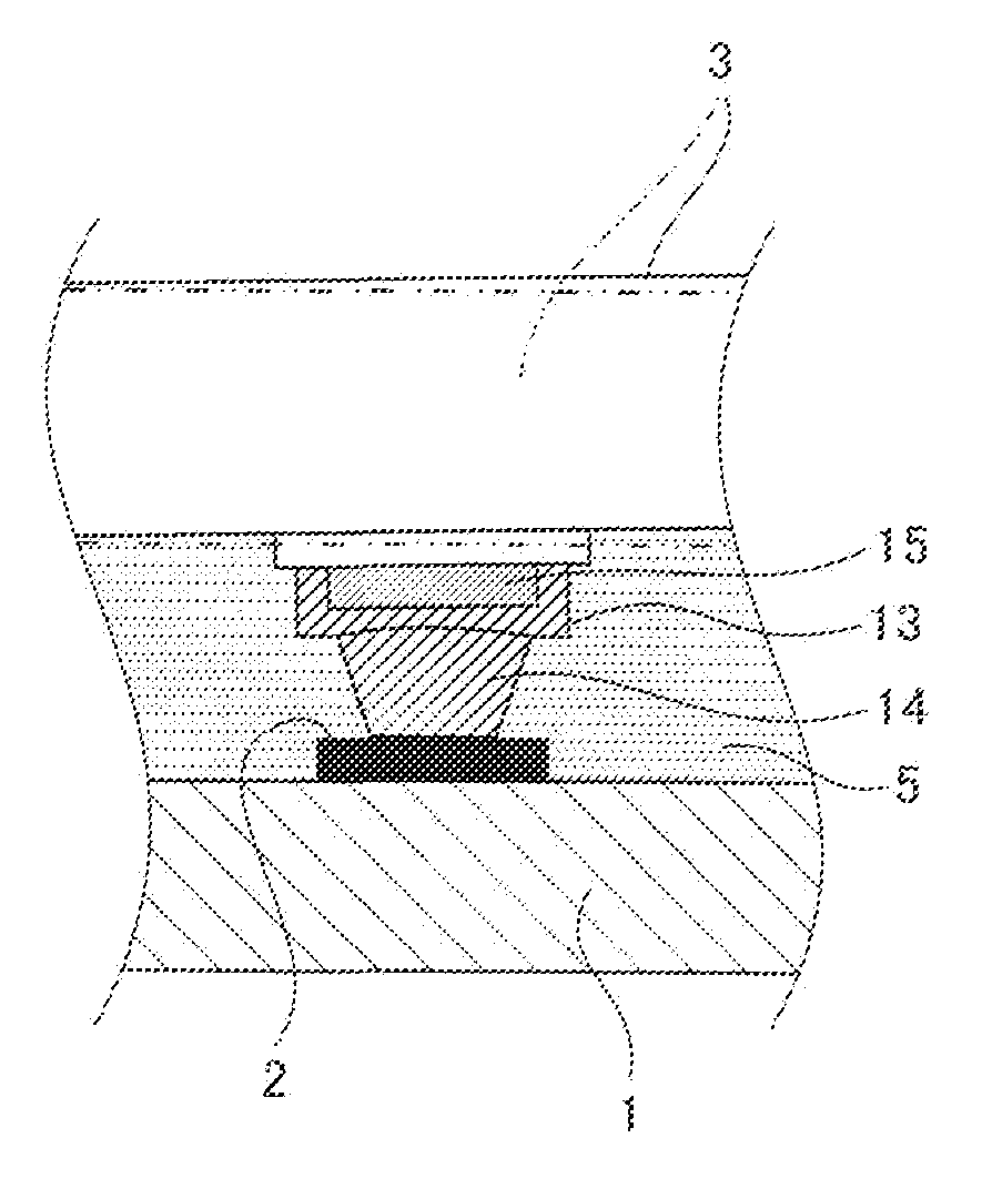
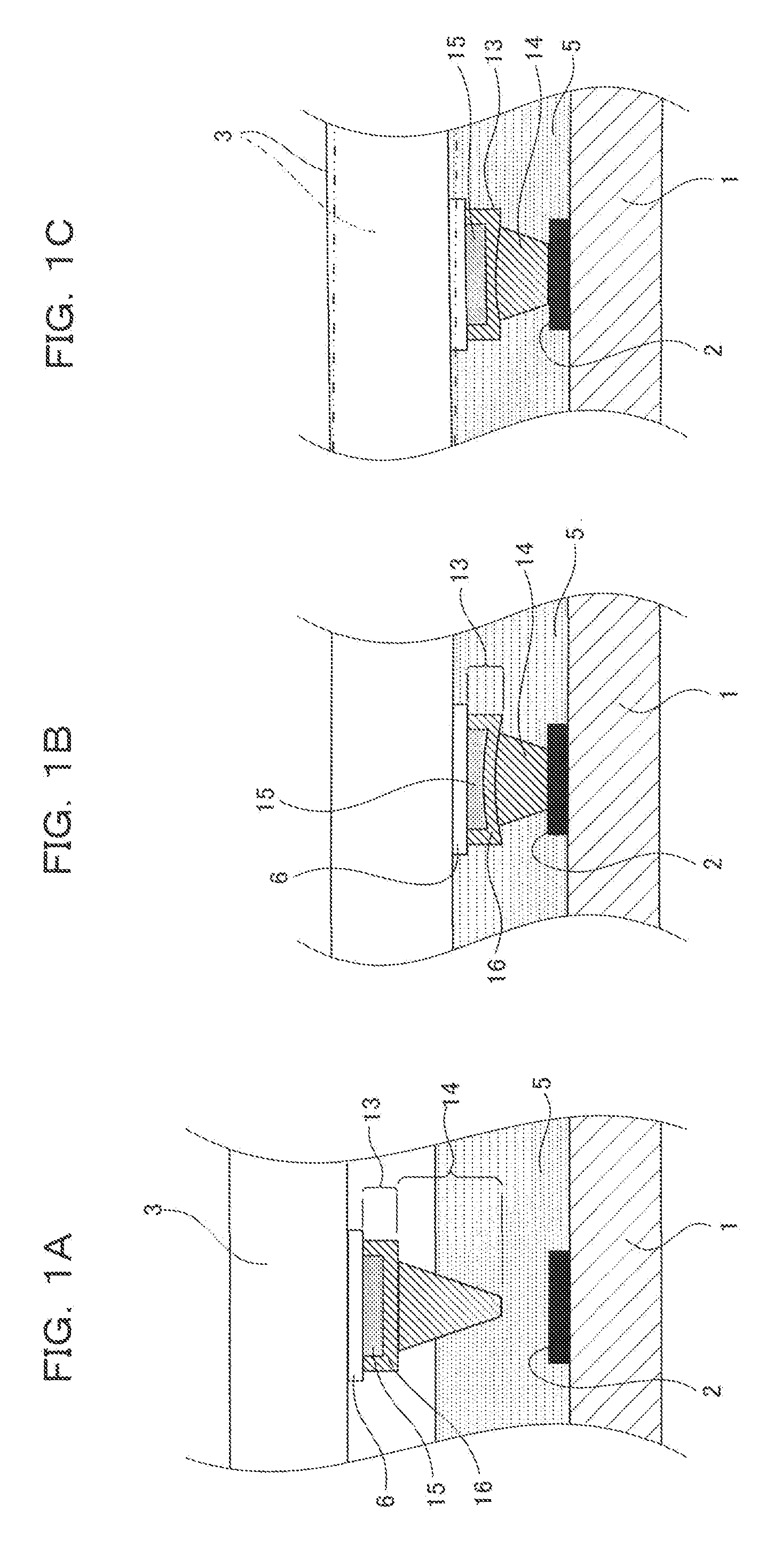
[0079]The core 15 of the table electrode 13 in the first reference mode is a flat disk-shaped, and the core 15 of the table electrode 13 in the second reference mode is in a ring shape, but as shown in FIG. 6A and FIG. 6B, it is also possible to provide a plurality of cores 15 having a smaller Young's modulus than a bump electrode 14 in a distributed fashion separated from one another on an electrode pad 6 formed on the surface of a semiconductor chip, and to cover the surfaces of the cores 15 and the gaps between the adjacent cores 15 with a conductive electrode 16.

[0080]By providing the plurality of cores 15 having a smaller Young's modulus than the bump electrode 14 in a distributed fashion separated from one another on the electrode pad 6 formed on the surface of the semiconductor chip, it is possible to distribute the stress due to the cores 15 being more liable to deform, compared to a case where core...

second embodiment

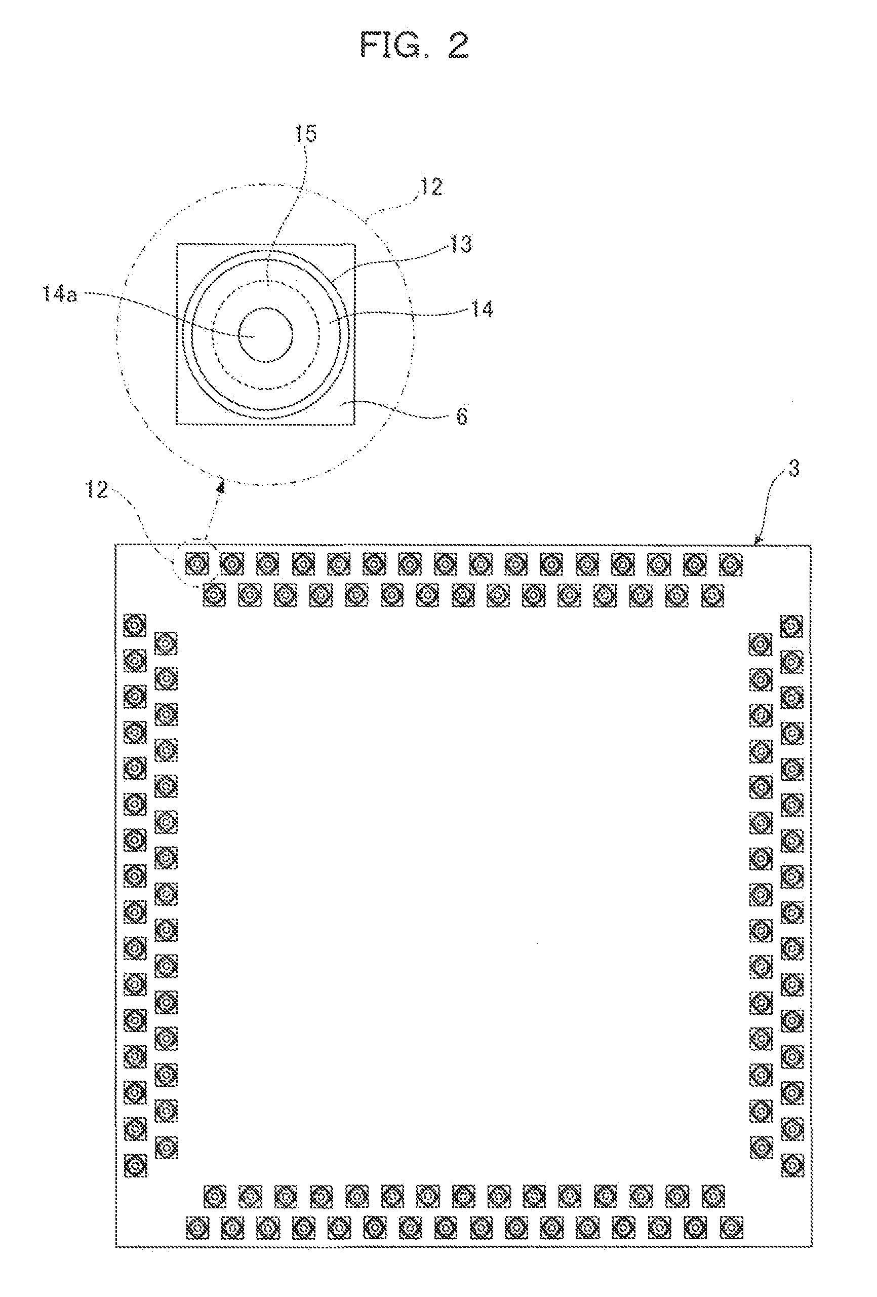
[0082]FIG. 8 shows the second embodiment of the present invention.

[0083]Similarly to FIG. 2, FIG. 8 shows a state immediately prior to flip-chip mounting a semiconductor chip 3 on a substrate 1. A plurality of electrodes 12 which are to form connection terminals of the chip on which an electrical circuit is built are formed on the surface of the semiconductor chip 3, the planar shape of the electrodes 12 following the outer shape of the rectangular semiconductor chip 3. In FIG. 8, in the electrodes 12 in corner portions 27 of the surface of the semiconductor chip, the total surface area of a plurality of cores 15 within a table electrode 13 is made greater than the total surface area of the plurality of cores 15 within the table electrode 13 of the electrode 12 located at the periphery of the corner portion 27.

[0084]In this way, furthermore, the nearer the position of the electrode 12 to the corner portion 27 which is subject to the effects of stress, the greater the total surface a...


PUM


Abstract

In this semiconductor chip 3, a table electrode 13 is interposed between a bump electrode 14 and an electrode pad 6. The table electrode 13 is formed by forming a plurality of cores 15 having a smaller Young's modulus than the bump electrode 14, on the electrode pad 6, and then covering the surfaces of the cores 15 with a conductive electrode 16. When the semiconductor chip 3 is flip-chip mounted, the bump electrode 14 is plastically deformed and the table electrode 13 is elastically deformed appropriately, thereby obtaining a good conductive state.

Description

TECHNICAL FIELD[0001]The invention relates to a semiconductor chip having a bump electrode.BACKGROUND ART[0002]In recent years, there has been a strong tendency toward reduced size in electronic devices, and progress has been made in enhancing functional integration and accelerating signal processing speeds. In association with this, the wiring of semiconductor chips has become thinner and the insulating layers and wiring layers of semiconductor chips have become more fragile. Furthermore, electrode pitches of 100 μm or less have come to be demanded.[0003]As shown in FIG. 10B, in a semiconductor device which has a semiconductor chip 3 flip-flop mounted onto a wire electrode 2 formed on a substrate 1, a bump electrode 4 formed on the surface of the semiconductor chip 3 is abutted against and electrically connected with the wire electrode 2 and in this state, a thermosetting resin 5 is cured and the position of the semiconductor chip 3 on the substrate 1 is fixed.[0004]More specifical...

Claims


Application Information

Patent Timeline
Patent Type & Authority Applications(United States)
IPC IPC(8): H01L23/488
CPCH01L24/05H01L2224/05554H01L2224/0401H01L2224/05599H01L2224/1147H01L2224/11472H01L2224/13099H01L2224/13144H01L2224/16225H01L2224/73204H01L2224/81001H01L2224/83192H01L2924/01004H01L2924/01005H01L2924/01014H01L2924/01022H01L2924/01028H01L2924/01029H01L2924/01046H01L2924/01078H01L2924/01079H01L2924/014H01L24/13H01L2924/01006H01L2924/01024H01L2924/01033H01L2224/16238H01L2224/81191H01L2924/00014H01L24/11H01L2224/05076H01L2224/05576H01L2224/02125H01L2924/00H01L2924/00012
Inventor TOMURA, YOSHIHIRONOBORI, KAZUHIROYAMADA, YUICHIROKUMAZAWA, KENTAROIWASE, TEPPEI
Owner PANASONIC CORP
Why Eureka
Try Eureka