

Semiconductor memory device
- Summary
- Abstract
- Description
- Claims
- Application Information
AI Technical Summary
Benefits of technology
Problems solved by technology
Method used
Image

Examples
first embodiment
[0022](Schematic Configuration of Nonvolatile Semiconductor Memory Device According to the First Embodiment)
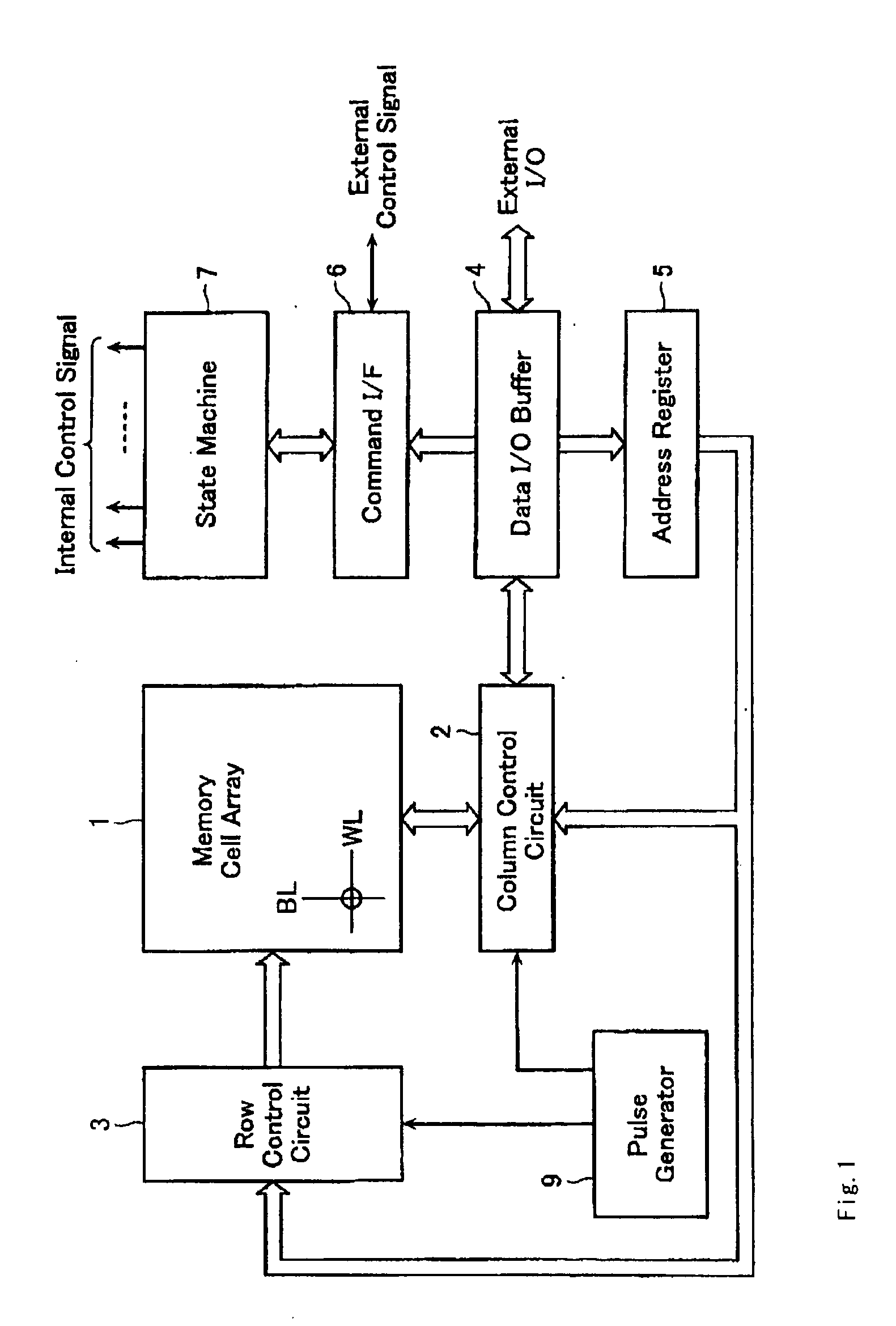
[0023]Referring to FIG. 1, first of all, the schematic configuration of a nonvolatile semiconductor memory device according to the first embodiment will be described below. FIG. 1 is a block diagram of the nonvolatile semiconductor memory device (nonvolatile memory) according to the first embodiment of the present invention.
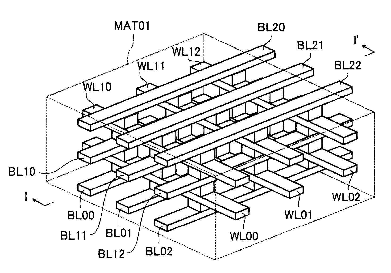
[0024]This nonvolatile semiconductor memory device comprises a memory cell array 1 in which the memory cells using a variable resistive element are arranged like a matrix. At the position adjacent to the memory cell array 1 in the direction of the bit line BL, a column control circuit 2 for controlling the bit line BL of the memory cell array 1 to erase data from the memory cell, write data into the memory cell and read data from the memory cell is provided. Also, at the position adjacent to the memory cell array 1 in the direction of the word line WL, a ro...
second embodiment
[0058](Write Operation of Nonvolatile Semiconductor Memory Device According to the Second Embodiment)
[0059]Referring now to FIGS. 11 and 12, the write operation of the nonvolatile semiconductor memory device according to the second embodiment will be described below. The nonvolatile semiconductor memory device according to the second embodiment performs the first write operation and the second write operation that are different from the first embodiment. FIG. 11 is a timing chart showing the first write operation according to the second embodiment. FIG. 12 is a timing chart showing the second write operation according to the second embodiment. In the nonvolatile semiconductor memory device according to the second embodiment, the same parts are designated by the same reference signs as in the first embodiment, and the explanation of the same parts is omitted.
[0060]Referring firstly to FIG. 11, the first write operation will be described below. First of all, the row control circuit 3 ...
PUM
 Abstract
Description
Claims
Application Information