
Solid-state imaging device and method for driving the same

a solid-state imaging and imaging device technology, applied in the direction of radio frequency controlled devices, instruments, television systems, etc., can solve the problems of difficult to decrease the voltage applied to the multiplication gate electrode, the pixel size is too large, and the potential in the charge barrier portion is difficult to decrease, so as to increase the electric charge and reduce the potential. the effect of the charge barrier portion

Active Publication Date: 2014-10-09
DENSO CORP
View PDF24 Cites 9 Cited by
  • Summary
  • Abstract
  • Description
  • Claims
  • Application Information

AI Technical Summary

Benefits of technology

The patent text describes a method for driving a charge barrier in a semiconductor device. By applying a low bias voltage during storage, the potential in the charge barrier decreases, allowing an electric charge to accumulate without moving it towards the surface of the semiconductor substrate. During the multiplication period, a high bias voltage is applied to increase the potential and accelerate the electric charge towards the insulation film, using avalanche multiplication to increase the electric charge. Overall, the method improves the efficiency and sensitivity of semiconductor devices.

Problems solved by technology

This caused the problem of increasing the pixel size and making it difficult to use a large number of pixels.
This makes it difficult to decrease a voltage applied to a multiplication gate electrode to acquire an electric field that enables the avalanche multiplication.

Method used


Image

  • Solid-state imaging device and method for driving the same
  • Solid-state imaging device and method for driving the same
  • Solid-state imaging device and method for driving the same

Examples


first embodiment

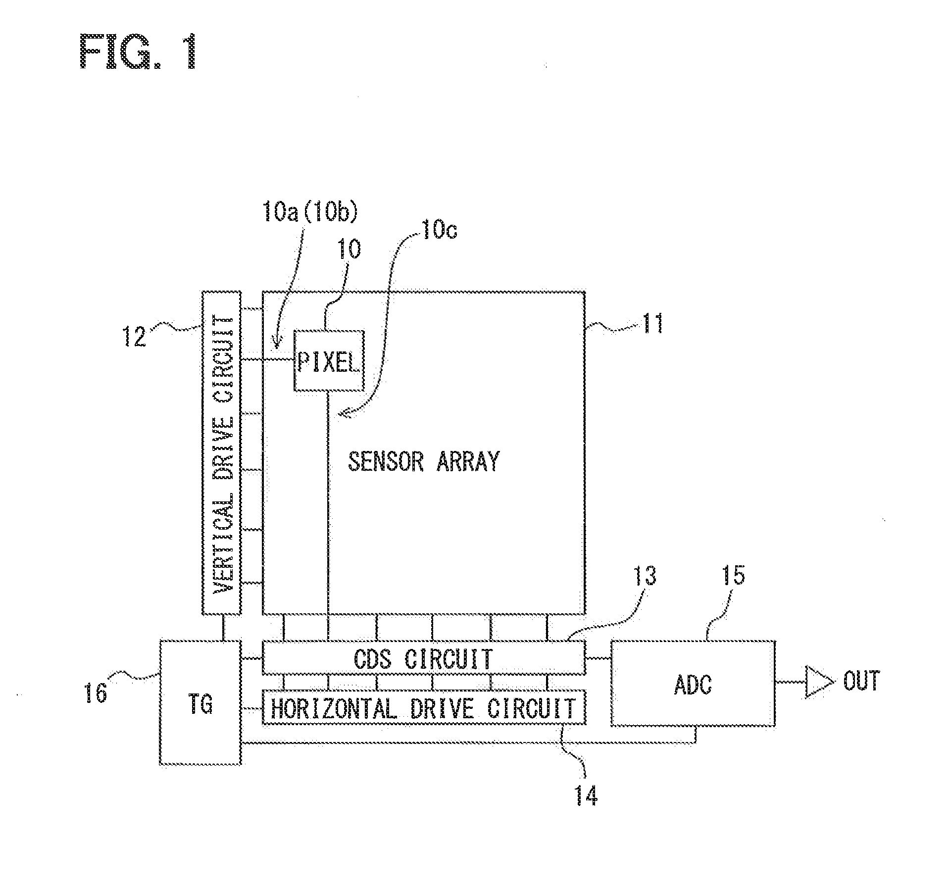
[0038]With reference to FIG. 1, the following describes a schematic configuration of the solid-state imaging device according to the embodiment.

[0039]The solid-state imaging device according to the embodiment configures a CMOS image sensor. As illustrated in FIG. 1, the solid-state imaging device includes a sensor array 11, a vertical drive circuit 12, a correlated double sampling (CDS) circuit 13, a horizontal drive circuit 14, an A / D converter circuit (ADC) 15, and a timing generator (TG) 16. The sensor array 11 includes multiple unit pixels (hereinafter simply referred to as pixels) arranged in a two-dimensional matrix.

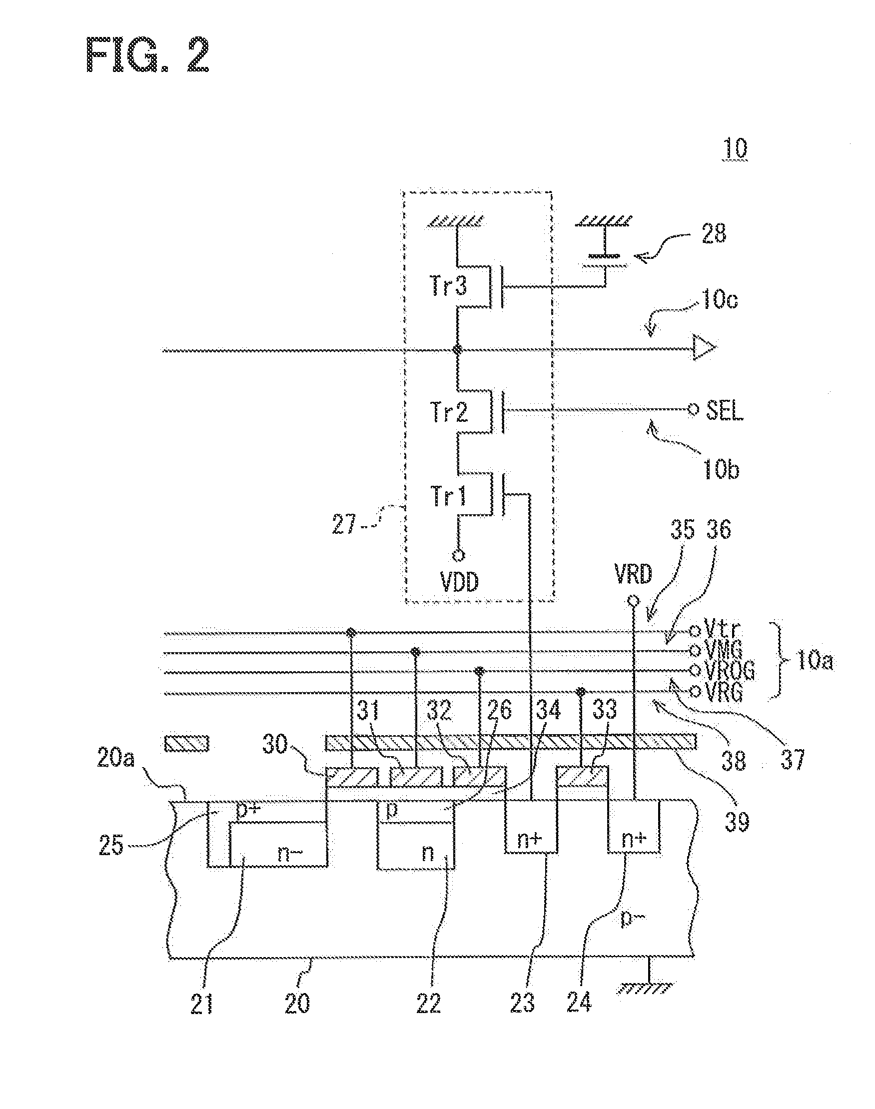
[0040]The unit pixel 10 includes at least such constituent elements as a photoelectric conversion portion, a charge holding portion, a floating diffusion (FD) portion, and a reset drain (RD) portion. The photoelectric conversion portion photoelectrically converts the incident light to store an electric charge. The charge holding portion receives the electric charge...

second embodiment

[0099]The first embodiment provides the example of forming the photoelectric conversion portion 21 and the charge holding portion 22 separately from each other. However, the present disclosure is not limited thereto. As illustrated in FIG. 16, for example, the photoelectric conversion portion 21 and the charge holding portion 22 may be formed adjacently to each other.

[0100]Such a configuration transfers an electric charge to the charge holding portion 22 from the time the photoelectric conversion portion 21 generates the electric charge according to photoelectric conversion. After a lapse of predetermined exposure time, applying clock pulse VMG to the multiplication gate electrode 31 multiplies the electric charge. The pixel 10 according to the second embodiment does not include the transfer gate electrode 30 unlike the first embodiment. The second embodiment can decrease the number of gate electrodes in the unit pixel 10 compared to the configuration according to the first embodime...

third embodiment

[0101]The first and second embodiments provide the examples of independently forming the photoelectric conversion portion 21 and the charge holding portion 22. However, the present disclosure is not limited thereto. As illustrated in FIG. 17, for example, the photoelectric conversion portion 21 and the charge holding portion 22 may be formed in the same region. In other words, the photoelectric conversion portion 21 is also used as the charge holding portion 22. This configuration forms the insulation film 34 and the multiplication gate electrode 31 over the photoelectric conversion portion 21.

[0102]In such a configuration, the hole accumulation layer 25 corresponds to the charge barrier portion 26. The potential positionally corresponding to the photoelectric conversion portion 21 in the thickness direction of the semiconductor substrate 20 approximately equals the potential positionally corresponding to the charge holding portion 22 according to the first embodiment. Applying cloc...


PUM

PropertyMeasurementUnit
bias voltageaaaaaaaaaa

Abstract

A solid-state imaging device includes: multiple pixels. Each pixel is arranged at a surface layer portion of a semiconductor substrate, and includes: a photoelectric conversion portion that converts light incident into an electric charge; a charge holding portion that stores the electric charge, and is arranged in the semiconductor substrate; a multiplication gate electrode that is capacitively coupled with the charge holding portion, and is arranged on the semiconductor substrate via an insulation film; and a charge barrier portion that is arranged between the charge holding portion and the insulation film, and has a higher impurity concentration than the semiconductor substrate.

Description

CROSS REFERENCE TO RELATED APPLICATION[0001]This application is based on Japanese Patent Applications No. 2012-26446 filed on Feb. 9, 2012, and No. 2013-10518 filed on Jan. 23, 2013, the disclosures of which are incorporated herein by reference.TECHNICAL FIELD[0002]The present disclosure relates to a solid-state imaging device having a gate electrode to amplify an electric charge and a method for driving the same.BACKGROUND ART[0003]Solid-state imaging devices using semiconductors are known as image sensors such as CCD image sensors and CMOS image sensors. The image sensors increase the number of pixels to generate finer images. As a result, reducing a light receiving area per pixel might decrease the sensitivity.[0004]To solve this problem, for example, Patent Document 1 proposes a solid-state imaging device having a gate electrode for avalanche multiplication between a photodiode portion to photoelectrically convert the incident light and a floating diffusion portion to convert an...

Claims


Application Information

Patent Timeline
Patent Type & Authority Applications(United States)
IPC IPC(8): H01L27/148H04N5/372
CPCH01L27/14614H04N5/37213H01L27/14806H01L27/14689H01L27/14623H04N25/713
Inventor TACHINO, YOSHIHIDEYAMASHIRO, TAKAHISAYOGO, YUKIAKI
Owner DENSO CORP
Features
  • Generate Ideas
  • Intellectual Property
  • Life Sciences
  • Materials
  • Tech Scout
  • Unparalleled Data Quality
  • Higher Quality Content
  • 60% Fewer Hallucinations
Learn More