

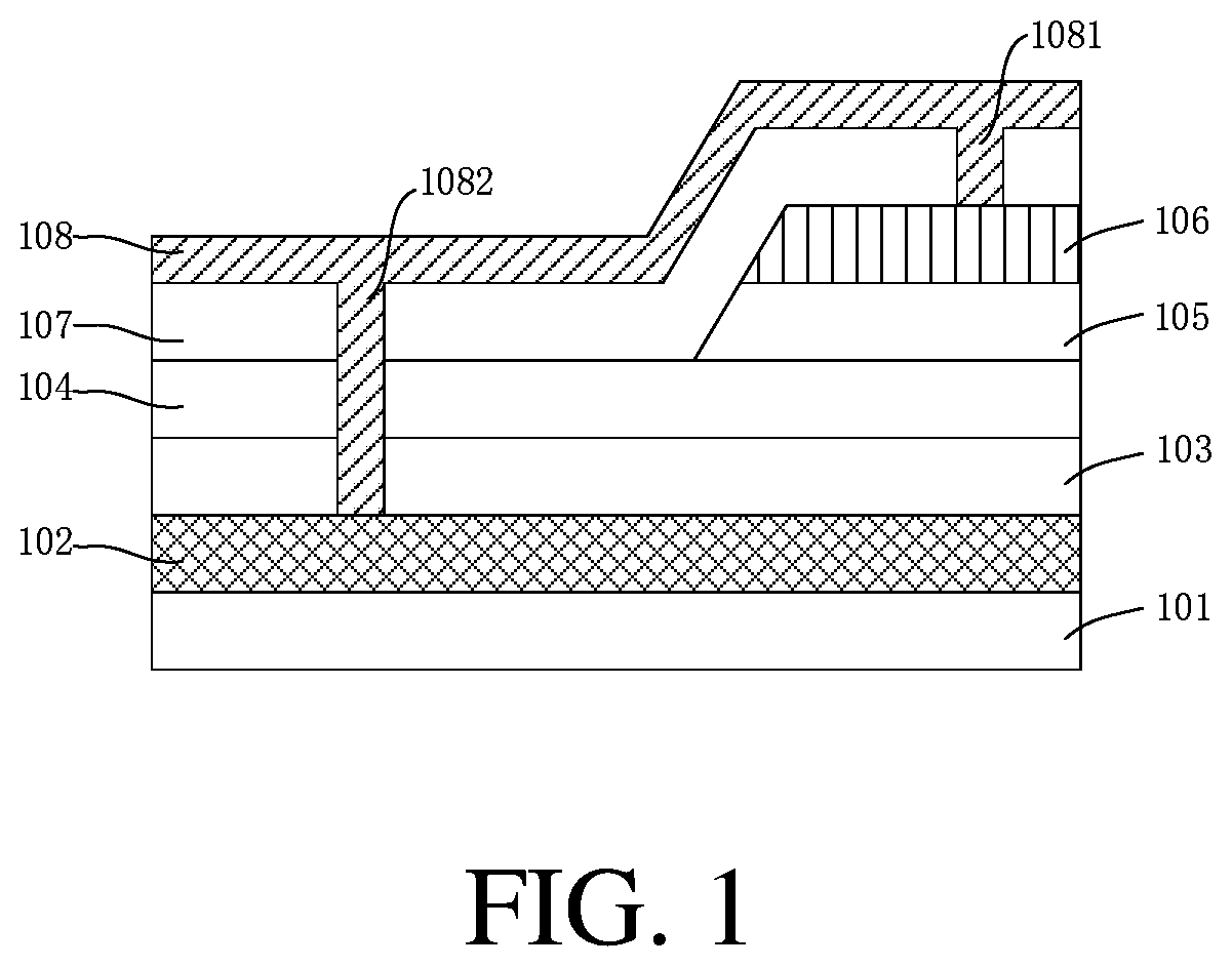
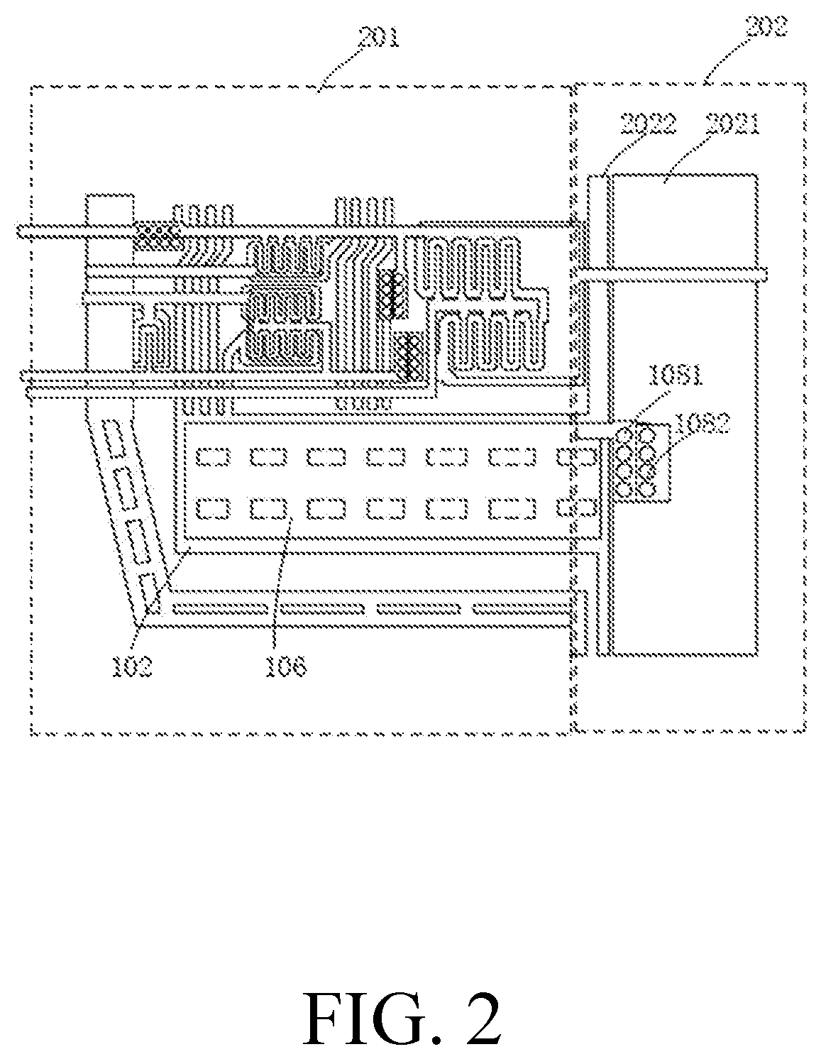
Array substrate and display panel
a display panel and substrate technology, applied in the field of array substrates and display panels, can solve the problems of large electric current, abnormal display panels, and risk of blast and injury, and achieve the effects of reducing the probability of electrostatic discharge, increasing the current conductive channel of the start pulse signal line, and improving the discharging rate of electric charges
- Summary
- Abstract
- Description
- Claims
- Application Information
AI Technical Summary
Benefits of technology
Problems solved by technology
Method used
Image

Examples
Embodiment Construction
[0031]The technical solutions in the embodiments of the present disclosure will be clearly and completely described below with reference to the drawings in the embodiments of the present disclosure. Obviously, the described embodiments are only a part of the embodiments of the present disclosure, but not all the embodiments. Based on the embodiments in the present disclosure, all other embodiments obtained by those skilled in the art without creative efforts are within the scope of the present disclosure.
[0032]The terms “first”, “second”, “third”, etc. (if present) in the specification, claims of the present disclosure, and the drawings are used to distinguish similar objects, and are not necessarily used to describe in a particular order or prioritization. it should be understood that the objects so described may be interchanged where appropriate. In addition, the term “comprises”, “have”, and their variations are intended to cover a non-exclusive inclusion.
[0033]In the specific em...
PUM
| Property | Measurement | Unit |
|---|---|---|
| area | aaaaa | aaaaa |
| dielectric | aaaaa | aaaaa |
| conductive | aaaaa | aaaaa |
Abstract
Description
Claims
Application Information