Plasma display panel and method of manufacturing the same

Inactive Publication Date: 2010-02-18
SAMSUNG SDI CO LTD
View PDF8 Cites 0 Cited by
  • Summary
  • Abstract
  • Description
  • Claims
  • Application Information

AI Technical Summary

Benefits of technology

[0008]It is therefore a feature of an embodiment to provide a highly efficient PDP that enables address driving with a low voltage.
[0009]It is therefore another feature of an embodiment to provide a PDP in which light-emitting efficiency is remarkably improved by realizing a high xenon (Xe) display.
[0010]It is therefore another feature of an embodiment to provide a high-quality PDP in which symmetric discharge is generated in each unit cell where a predetermined image is realized, and thus, an overall display quality of the PDP is improved.
[0011]It is therefore another feature of an embodiment to provide a PDP in which consumption of reactive power, which does not contribute to light emitting luminance, may be reduced and discharge intervention between neighboring cells is prevented.

Problems solved by technology

Moreover, as the PDP rapidly develops to a full high definition (HD) level, the number of the discharge cells increases in geometrical proportion, increasing power consumption by a circuit unit in proportion to the number of address electrodes allocated to each discharge cell.
A relatively high address voltage, however, is required for discharge initiation in such a high Xe display, further increasing power consumption.

Method used


Image

  • Plasma display panel and method of manufacturing the same
  • Plasma display panel and method of manufacturing the same
  • Plasma display panel and method of manufacturing the same

Examples


Embodiment Construction

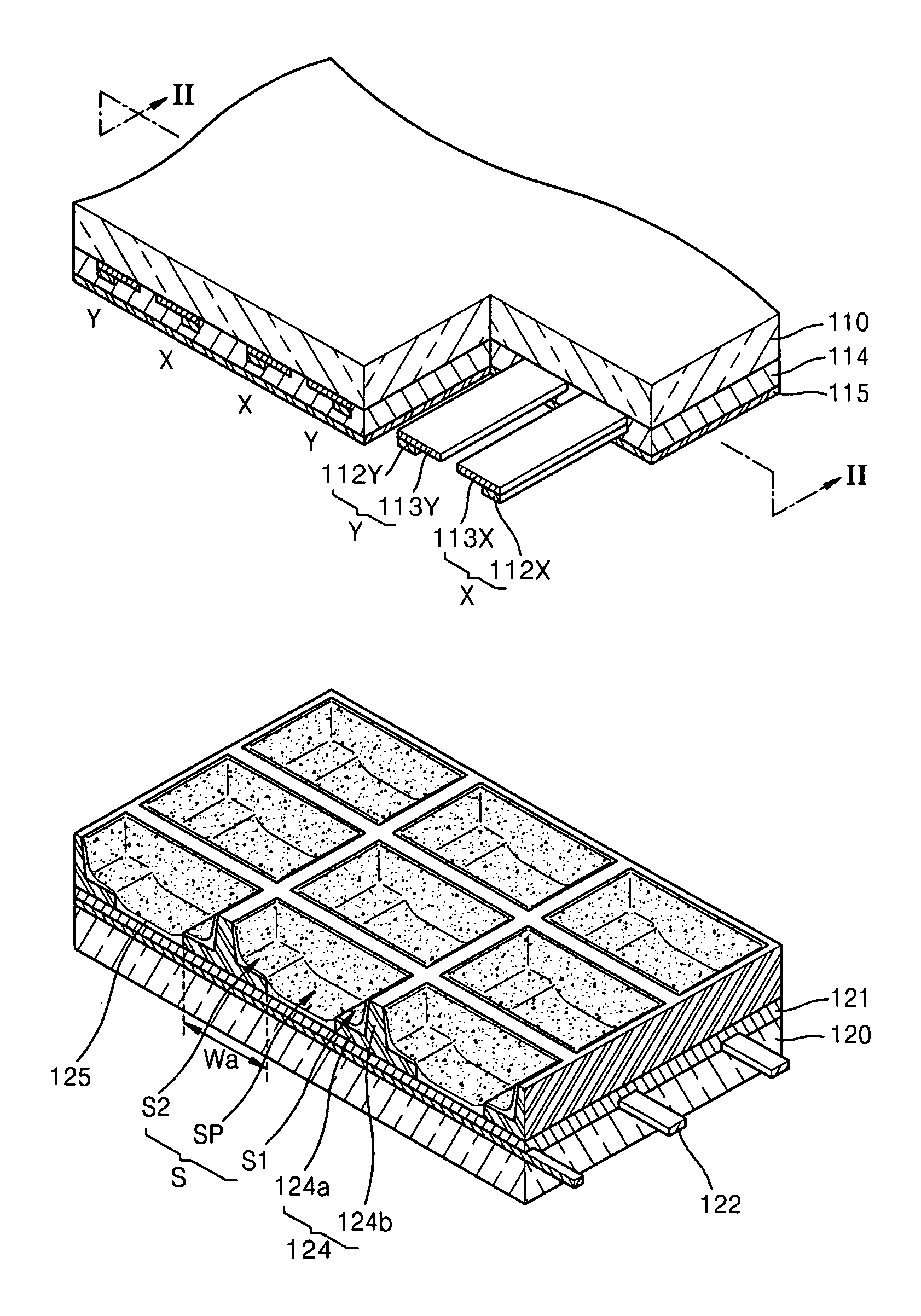
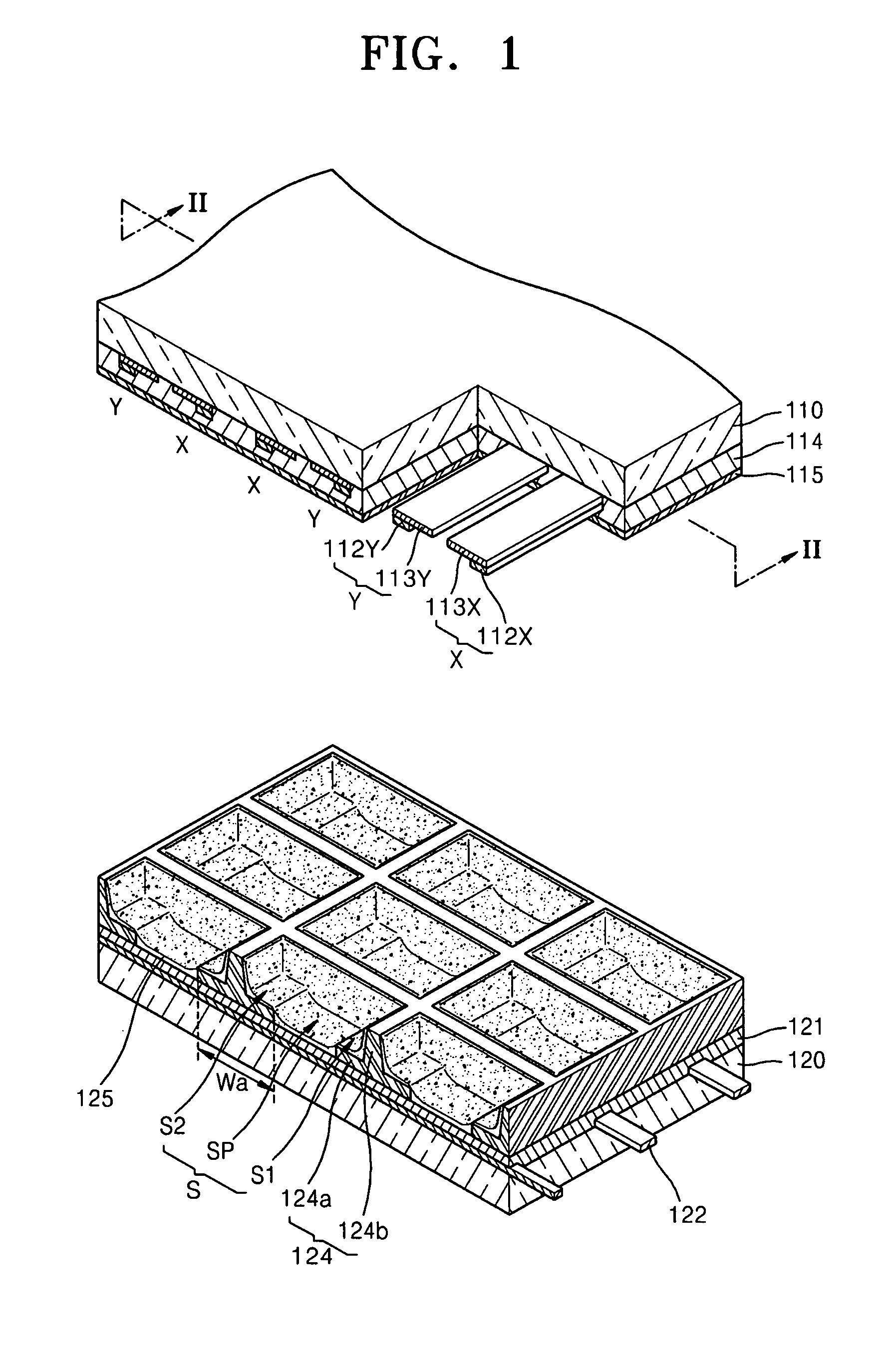
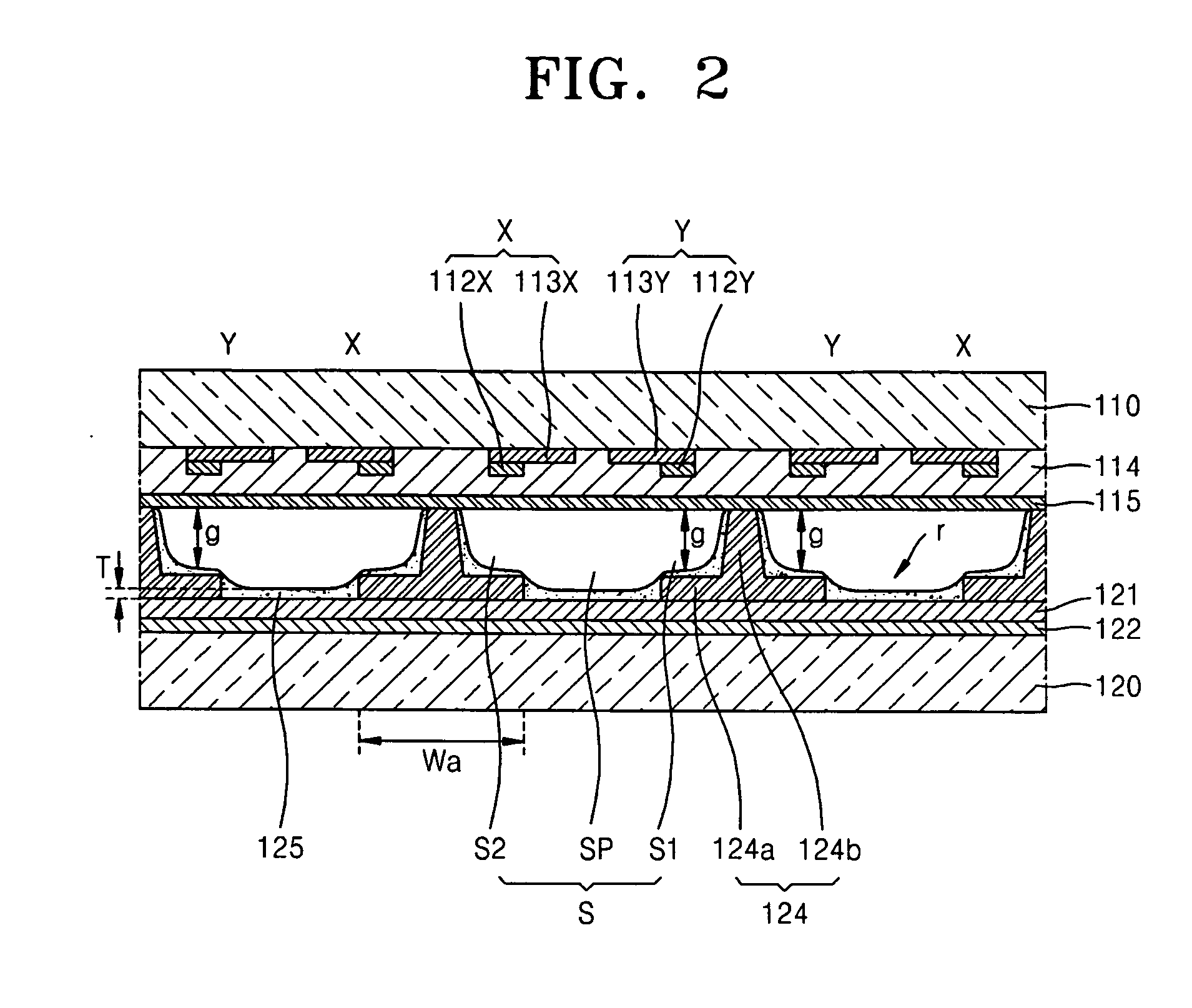
[0046]Korean Patent Application No. 10-2008-0078719, filed on Aug. 12, 2008, in the Korean Intellectual Property Office, and entitled: “Plasma Display Panel,” is incorporated by reference herein in its entirety.

[0047]Example embodiments will now be described more fully hereinafter with reference to the accompanying drawings; however, they may be embodied in different forms and should not be construed as limited to the embodiments set forth herein. Rather, these embodiments are provided so that this disclosure will be thorough and complete, and will fully convey the scope of the invention to those skilled in the art.

[0048]In the drawing figures, the dimensions of layers and regions may be exaggerated for clarity of illustration. It will also be understood that when a layer or element is referred to as being “on” another layer or substrate, it can be directly on the other layer or substrate, or intervening layers may also be present. Further, it will be understood that when a layer is...


PUM


Abstract

A plasma display panel (PDP) including a front substrate and a rear substrate facing each other, a partition wall interposed between the front substrate and the rear substrate to define a plurality of unit cells, each unit cell including a main discharge space, an auxiliary discharge space, and a step space, the auxiliary discharge space and the step space being on opposite sides of the main discharge space along a stepped sidewall of the partition wall, pairs of scanning and sustain electrodes arranged adjacent the auxiliary discharge spaces and to the step spaces, respectively, address electrodes extending to cross the scanning electrodes at a location adjacent to the auxiliary discharge spaces, a phosphor layer formed at least in the main discharge spaces, and discharge gas filling the unit cell.

Description

BACKGROUND[0001]1. Field[0002]Embodiments relate to a plasma display panel (PDP) and method of manufacturing the same and, more particularly, to a PDP in which an address discharge path is shortened so that low-voltage addressing is possible, and having symmetric discharge in each unit cell realizing a predetermined image, thereby improving overall displaying quality.[0003]2. Description of the Related Art[0004]In a PDP, a plurality of discharge cells arranged in a matrix form is interposed between upper and lower substrates facing each other. Discharge electrodes including pairs of scanning electrodes and sustain electrodes, which cause mutual discharge, and a plurality of address electrodes are disposed on the substrates. An appropriate discharge gas is injected between the substrates, a predetermined discharge pulse is applied between discharge electrodes, fluorescent substances applied within the plurality of discharge cells are excited, and a predetermined image is realized usi...

Claims


Application Information

Patent Timeline
IPC IPC(8): H01J17/49H01J11/12H01J11/36H01J11/40
CPCH01J11/12H01J11/36H01J2211/363H01J2211/361H01J11/40H01J11/34
Inventor SON, SEUNG-HYUN
Owner SAMSUNG SDI CO LTD
Why Eureka
Try Eureka