Semiconductor die support in an offset die stack

Inactive Publication Date: 2010-02-25
SANDISK TECH LLC
View PDF7 Cites 29 Cited by
  • Summary
  • Abstract
  • Description
  • Claims
  • Application Information

AI Technical Summary

Benefits of technology

[0052]Referring now to the side view of FIG. 14, a second semiconductor die 340 may next be mounted atop the first semiconductor die 320 using an adhesive die attach layer 342. The loop 364 may be slightly compressed by the second die 340 when it is mounted on the die stack, but the balcony loop 360 provides structural support for overhanging edge 344 of die 340. This structural support is sufficient to withstand the pressure exerted on edge 344 during the subsequent wire bonding process. As the balcony loop 360 is conductive and is in contact with both contact pads 304a, 306 and the underside of die 340, the contact pads 304a and 306 may be electrically grounded pads. Thus, electrical shorting is prevented. It is understood that a layer of dielectric may be provided on the underside of die 340 instead of or in addition to adhesive die attach layer 342

Problems solved by technology

In addition to the height of the bond wires 30 themselves, additional space must be left above the bond wires, as contact of the bond wires 30 of one die with the next die above may result in an electrical short.
One problem in conventional semiconductor packages is that, when the wire bonding capillary contacts the upper

Method used


Image

  • Semiconductor die support in an offset die stack
  • Semiconductor die support in an offset die stack
  • Semiconductor die support in an offset die stack

Examples


Example

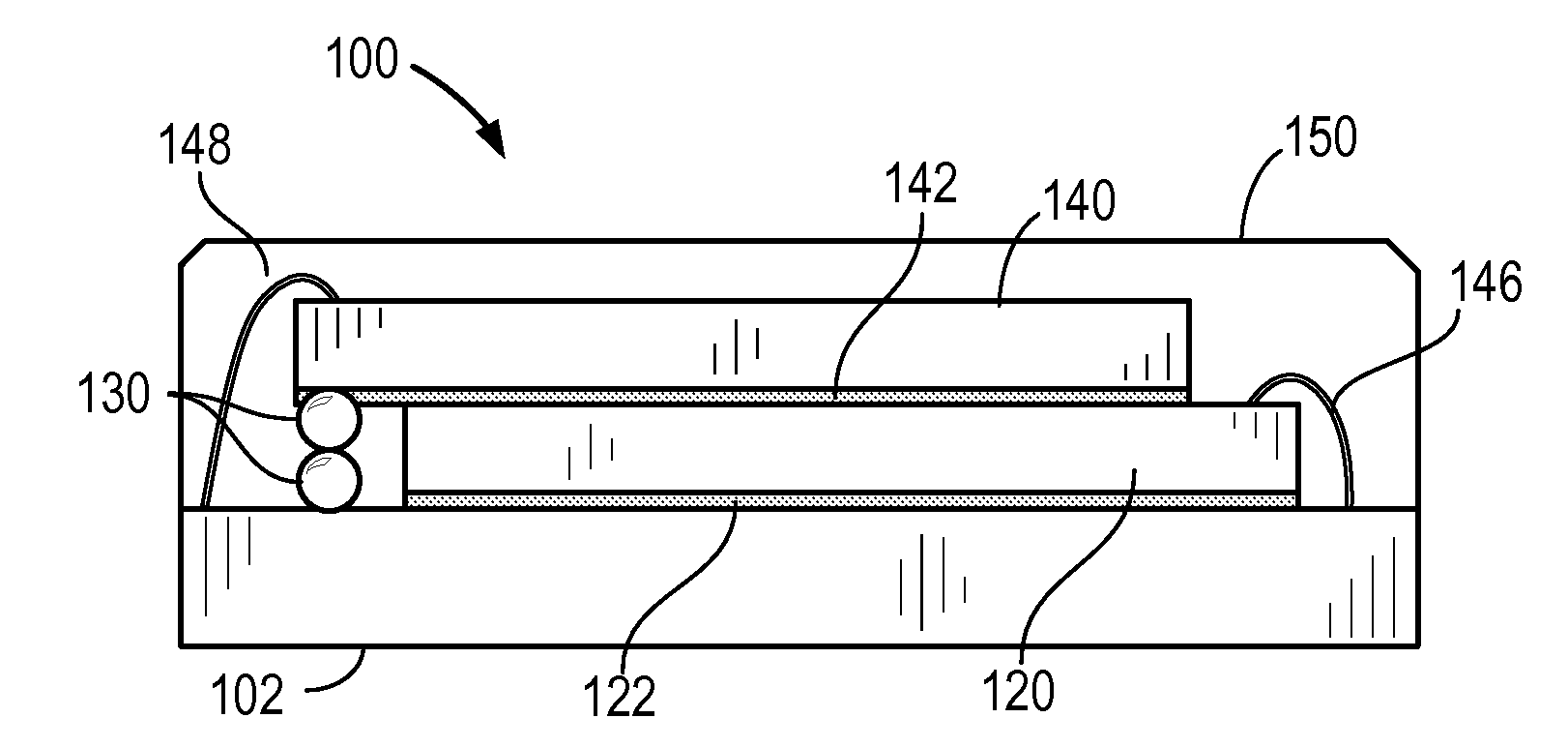
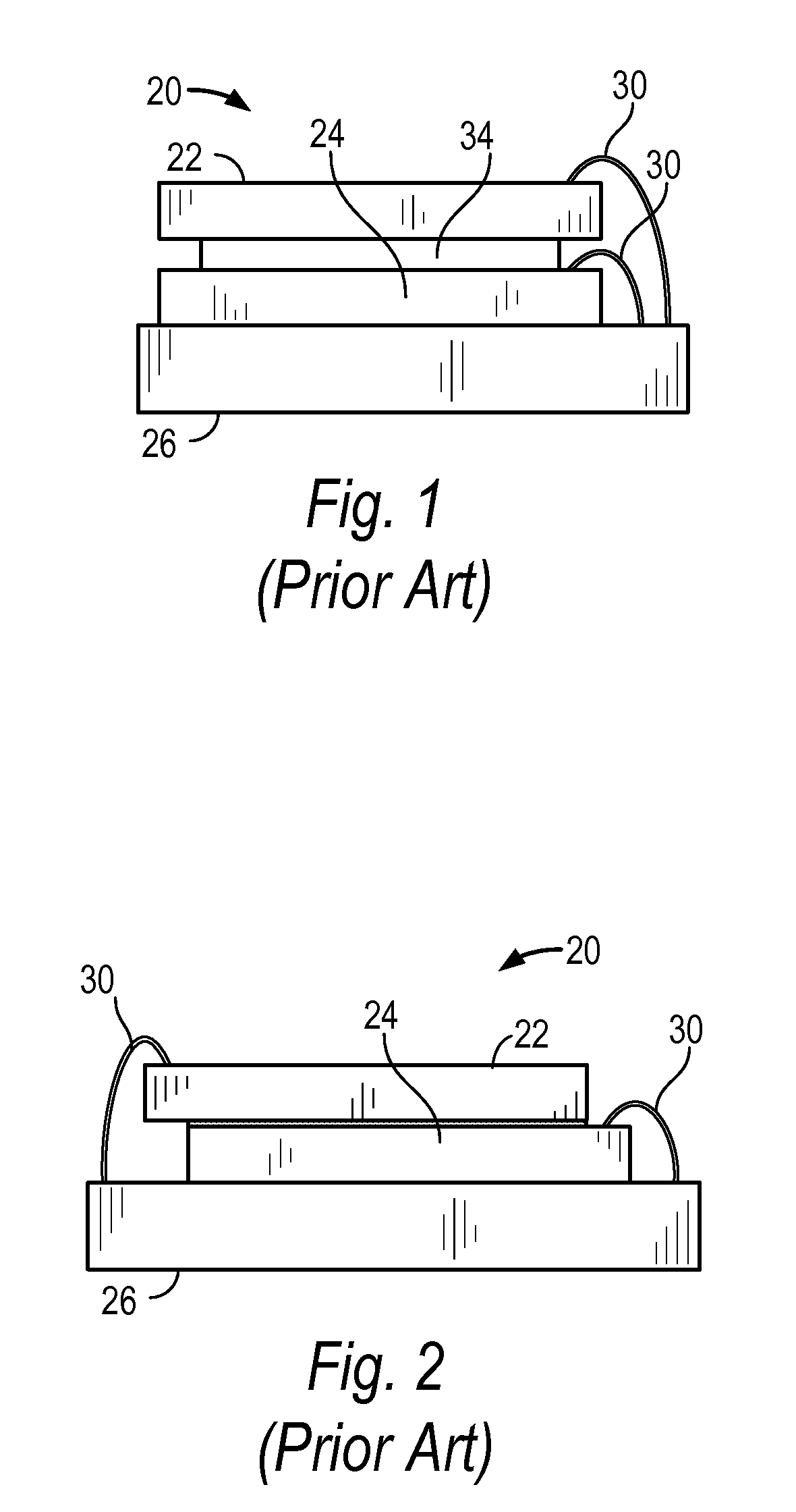
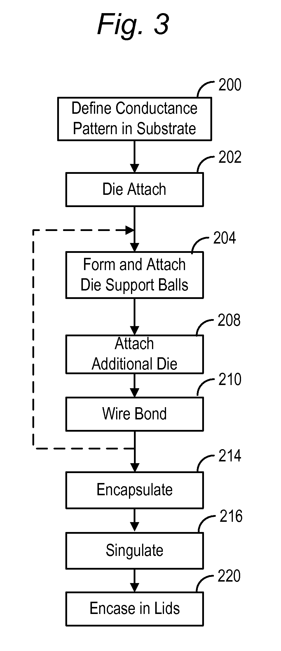
[0030]Embodiments will now be described with reference to FIGS. 3 through 15, which relate to a semiconductor package and methods of forming same. It is understood that the present invention may be embodied in many different forms and should not be construed as being limited to the embodiments set forth herein. Rather, these embodiments are provided so that this disclosure will be thorough and complete and will fully convey the invention to those skilled in the art. Indeed, the invention is intended to cover alternatives, modifications and equivalents of these embodiments, which are included within the scope and spirit of the invention as defined by the appended claims. Furthermore, in the following detailed description of the present invention, numerous specific details are set forth in order to provide a thorough understanding of the present invention. However, it will be clear to those of ordinary skill in the art that the present invention may be practiced without such specific ...


PUM


Abstract

A semiconductor device is disclosed including a support structure for supporting an edge of a semiconductor die that is not supported on the substrate or semiconductor die below. In embodiments, the semiconductor device may in general include a substrate having a plurality of contact pads, a first semiconductor die mounted on the substrate, and a second semiconductor die mounted on the first semiconductor die in an offset configuration so that an edge of the second semiconductor die overhangs the first semiconductor die. A support structure may be affixed to one or more of the contact pads beneath the overhanging edge to support the overhanging edge during a wire bonding process which exerts a downward force on the overhanging edge.

Description

BACKGROUND OF THE INVENTION[0001]1. Field of the Invention[0002]Embodiments of the present invention relate to a low profile semiconductor device and method of fabricating same.[0003]2. Description of the Related Art[0004]The strong growth in demand for portable consumer electronics is driving the need for high-capacity storage devices. Non-volatile semiconductor memory devices, such as flash memory storage cards, are becoming widely used to meet the ever-growing demands on digital information storage and exchange. Their portability, versatility and rugged design, along with their high reliability and large capacity, have made such memory devices ideal for use in a wide variety of electronic devices, including for example digital cameras, digital music players, video game consoles, PDAs and cellular telephones.[0005]While a wide variety of packaging configurations are known, flash memory storage cards may in general be fabricated as system-in-a-package (SiP) or multichip modules (MC...

Claims


Application Information

Patent Timeline
IPC IPC(8): H01L23/49
CPCH01L24/32H01L24/33H01L2224/48247H01L2224/32245H01L2924/0665H01L2924/014H01L2924/01322H01L2224/2919H01L2924/19107H01L2924/1815H01L2924/01082H01L2924/01079H01L2924/01078H01L2924/01047H01L2924/01033H01L2924/01029H01L2924/01013H01L2924/01004H01L2225/06586H01L2225/06562H01L2225/0651H01L2224/97H01L2224/85186H01L24/83H01L24/92H01L24/97H01L25/0657H01L2224/32145H01L2224/32225H01L2224/48091H01L2224/48225H01L2224/48227H01L2224/73265H01L2224/83191H01L2224/838H01L2224/85181H01L2924/00014H01L2224/85H01L2224/83H01L2924/00H01L2924/3512H01L2924/00012H01L2224/92247H01L2924/181H01L2224/05554H01L24/73H01L2224/023H01L2924/0001H01L23/12
Inventor CHIU, CHIN-TIENTAKIAR, HEMXI, JIA QING
Owner SANDISK TECH LLC
Why Eureka
Try Eureka