Circuit board structure comprising an electrical component and a method for manufacturing a circuit board structure comprising an electrical component

Active Publication Date: 2010-02-25
IMBERATEK LLC
View PDF17 Cites 9 Cited by
  • Summary
  • Abstract
  • Description
  • Claims
  • Application Information

AI Technical Summary

Benefits of technology

[0021]When the holes through the plane-like layer and/or the conductive pattern are formed before the electrical components are attached to the circuit board structure, the holes may be used for component alignment. Thereby, component terminals may be easily and accurately aligned with the holes in the plane-like layer, and any systematic errors in the positioning of the holes do not affect the position of the component terminals in relation to the holes. This enables more reliable electrical contacts between the component terminals and the conductive pattern. In addition, the components may be positioned in a denser fashion on the circuit board, and the pitch of the components becomes finer, which enables the manufacture of even complex circuits.
[0022]The manufacturability and yield of circuit boards manufactured using the method in accordance with the invention may also

Problems solved by technology

A further key issue is the improvement of the yield and reliability of the manufacturing process.
Such mutual positioning of wire bonds, components and the conductive pattern makes an encapsulation of the integrated circuit more difficult and increases the risk of the conductive pattern and the elect

Method used


Image

  • Circuit board structure comprising an electrical component and a method for manufacturing a circuit board structure comprising an electrical component
  • Circuit board structure comprising an electrical component and a method for manufacturing a circuit board structure comprising an electrical component
  • Circuit board structure comprising an electrical component and a method for manufacturing a circuit board structure comprising an electrical component

Examples


Embodiment Construction

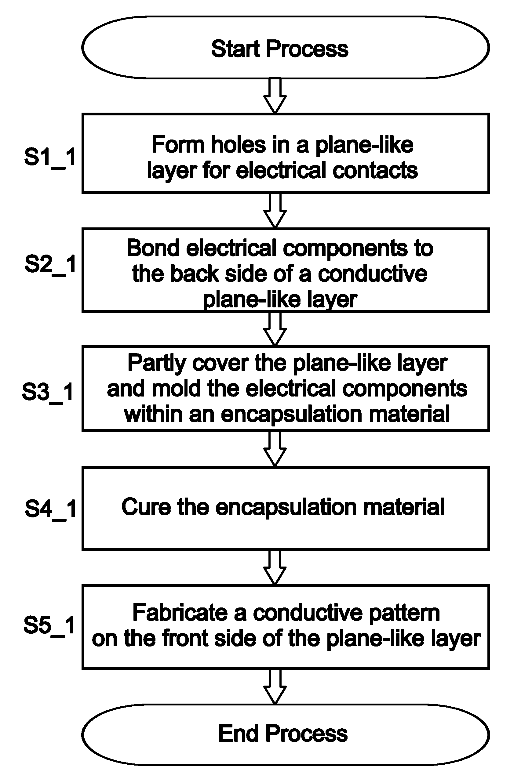
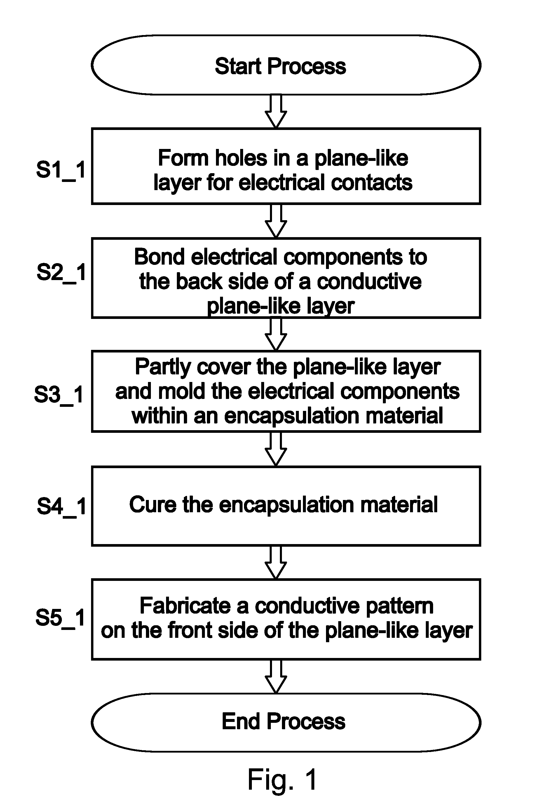
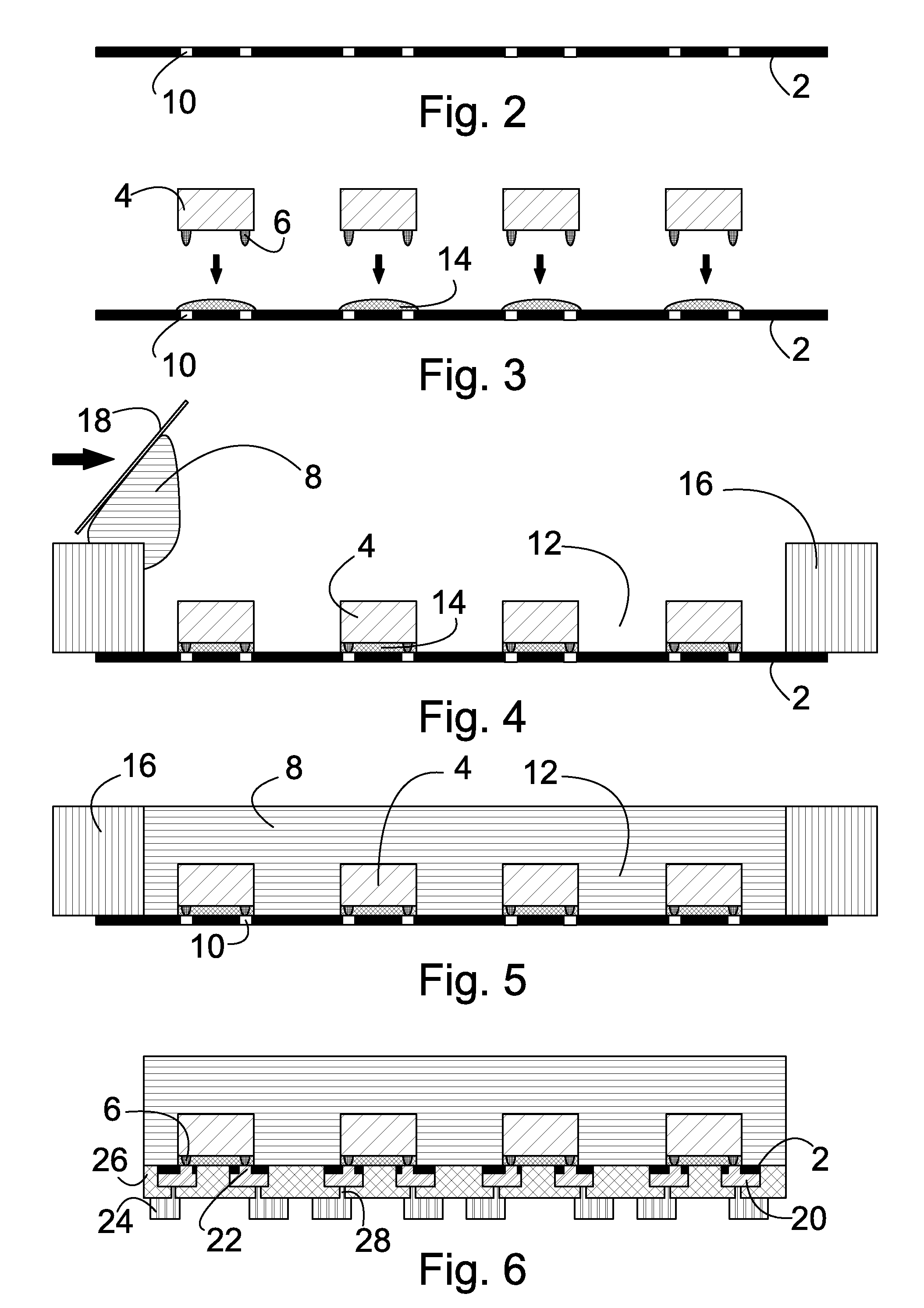
[0028]In the following, the invention is described by means of examples by reference to the following drawings, where

[0029]FIG. 1 shows a flow chart of an embodiment of the method in accordance with the invention,

[0030]FIGS. 2 to 6 show a series of views schematically presenting the method in accordance with the flow chart shown in FIG. 1,

[0031]FIG. 7 shows a flow chart of an embodiment of the method in accordance with the invention,

[0032]FIGS. 8 to 13 show a series of views schematically presenting the method in accordance with the flow chart shown in FIG. 7,

[0033]FIG. 14 shows a flow chart of an embodiment of the method in accordance with the invention,

[0034]FIGS. 15 to 19 show a series of views schematically presenting the method in accordance with the flow chart shown in FIG. 14,

[0035]FIG. 20 shows a flow chart of an embodiment of the method in accordance with the invention, and

[0036]FIGS. 21 to 26 show a series of views schematically presenting the method in accordance with the...


PUM

PropertyMeasurementUnit
Electrical conductoraaaaaaaaaa

Abstract

A circuit board structure and a method for manufacturing a circuit board structure comprising an electrical component. The method comprises the steps of fabricating a conductive pattern on the surface of an essentially plane-like layer on the back side of the plane-like layer, and forming an electrical contact between at least one electrical component and the conductive pattern. The method further comprises the steps of attaching at least one electrical component to the back side of the plane-like layer after the fabrication of the conductive pattern, molding encapsulation material on the back side of the plane-like layer so that the encapsulation material at least partly encloses the at least one electrical component attached to the back side of the plane-like layer, and forming holes through the conductive pattern at positions where terminals of the electrical components attached to the back side of the plane-like layer become positioned when the electrical component is attached to the circuit board structure.

Description

[0001]This application claims benefit of Serial No. 20085790, filed 25 Aug. 2008 in Finland and which application(s) are incorporated herein by reference. To the extent appropriate, a claim of priority is made to each of the above disclosed applications.TECHNICAL FIELD[0002]The invention relates to electronics packaging technology. Particularly, the invention relates to a circuit board structure and a method for manufacturing a circuit board and for encapsulating an electrical component on the circuit board.BACKGROUND OF THE INVENTION[0003]The development of circuit board manufacturing methods and packaging methods aims at, among other things, a denser layout of electrical components on the circuit board, a thinner circuit board structure, and improving the mechanical, electrical, and thermal properties of the circuit board. A further key issue is the improvement of the yield and reliability of the manufacturing process.[0004]Patent specification U.S. Pat. No. 5,192,682 discloses a ...

Claims


Application Information

Patent Timeline
IPC IPC(8): H05K1/18H05K3/32
CPCH01L24/18Y10T29/4913H01L24/97H01L2224/18H01L2224/73204H01L2224/82039H01L2224/83192H01L2224/92H01L2224/97H01L2924/01013H01L2924/01029H01L2924/01046H01L2924/01078H01L2924/01079H01L2924/14H01L2924/19041H01L2924/19043H01L2924/3025H05K1/187H05K1/188H05K3/205H05K3/305H05K2201/0355H05K2201/0969H05K2201/10674H05K2203/1469H01L24/82Y10T29/49146Y10T29/49117Y10T29/49139H01L2924/1461H01L2924/18162H01L2924/12041H01L2924/01033H01L2224/81H01L2224/82H01L2924/00H01L21/568H01L24/19H01L24/96H01L2224/81005H01L2924/181H01L2924/19105H01L2924/00012H01L21/56H01L23/3121H05K3/284
Inventor PALM, PETTERIWARIS, TUOMAS
Owner IMBERATEK LLC
Why Eureka
Try Eureka