Method for manufacturing photoelectric conversion device

Inactive Publication Date: 2010-02-25
SEMICON ENERGY LAB CO LTD
View PDF22 Cites 31 Cited by
  • Summary
  • Abstract
  • Description
  • Claims
  • Application Information

AI Technical Summary

Benefits of technology

[0026]A photoelectric conversion device with a higher photoelectric conversion efficiency can be manufactured with reduced consumption of resources because a layer conducting photoelectric conversion is formed by increasing the thickness of a single crystal silicon layer having reduced crystal defects with a crystal epitaxial growth technique using an atmospheric pressure plasma CVD method. Moreover, the consumption of single crystal silicon, which is a raw material, ca

Problems solved by technology

However, by a technique such as a hydrogen ion implantation separation method in which a thin superficial layer of a single crystal silicon substrate is separated as a single crystal silicon layer, generation of crystal defects in a hydrogen ion implantation process or separation process cannot be prevented.
However, if there is a crystal defect in a single crystal s

Method used


Image

  • Method for manufacturing photoelectric conversion device
  • Method for manufacturing photoelectric conversion device
  • Method for manufacturing photoelectric conversion device

Examples


embodiment mode 1

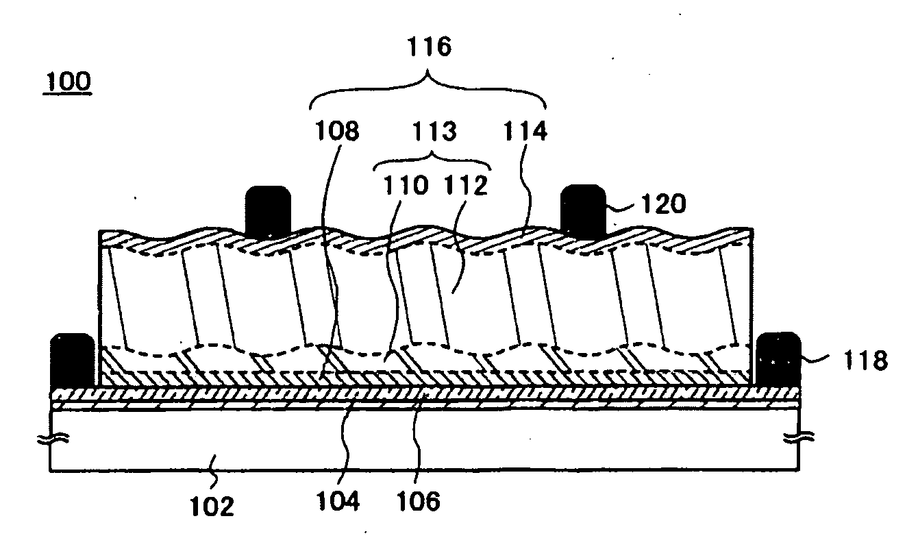
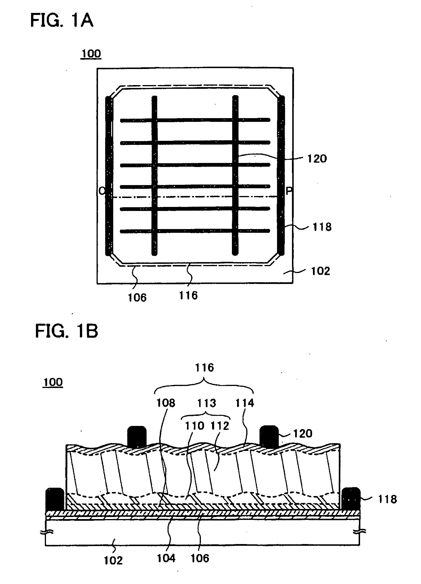
[0049]FIG. 1A is a schematic top diagram and FIG. 1B is a schematic cross-sectional diagram of a photoelectric conversion device 100 according to the present invention. Note that FIG. 1B is an example of a cross-sectional view along line O-P in FIG. 1A.

[0050]The photoelectric conversion device 100 described in this embodiment mode includes a unit cell 116 having a single crystal silicon layer over the supporting substrate 102. The unit cell 116 is provided with a first electrode 106 on the supporting substrate 102 side and with a second electrode 120 on an opposite surface from the supporting substrate 102 side. The unit cell 116 is sandwiched between the first electrode 106 and the second electrode 120. In addition, an insulating layer 104 is provided between the supporting substrate 102 and the unit cell 116. The first electrode 106 is provided between the unit cell 116 and the insulating layer 104. The second electrode 120 is provided on the opposite surface of the unit cell 116 ...

embodiment mode 2

[0155]In this embodiment mode, a method for manufacturing a photoelectric conversion device which is different from the method described in the above embodiment mode is described. In the above embodiment mode, an example is given in which crystal defects in the first single crystal silicon layer 110 which is formed of a slice of the single crystal silicon substrate 101 are repaired by laser treatment. In this embodiment mode, a method is described in which a surface of the first single crystal silicon layer 110 is removed to reduce crystal defects. Note that other structures are based on the description in the above embodiment mode and the description thereof is omitted here.

[0156]By performing etching treatment or polishing treatment on a surface which is the separation plane of the first single crystal silicon layer 110, which is a thin slice of the single crystal silicon substrate 101, crystal defects of the surface which is the separation plane can be eliminated.

[0157]For exampl...

embodiment mode 3

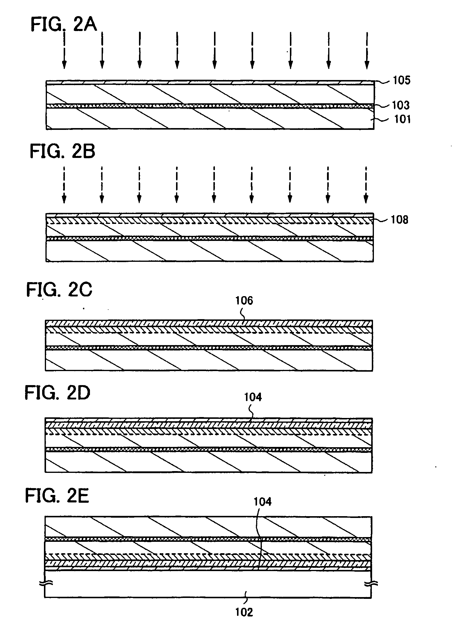
[0161]In this embodiment mode, a method for manufacturing a photoelectric conversion device which is different from the methods described in the above embodiment modes is described with reference to FIGS. 10A to 10D, FIGS. 11A to 11D, and FIGS. 12A to 12D. In specific, a method for forming the fragile layer 103 and the first impurity silicon layer 108 in the single crystal silicon substrate 101, and forming the first electrode 106, and the insulating layer 104 over the single crystal silicon substrate 101 is described. Note that other structures are based on the description in the above embodiment modes and the description thereof is omitted here.

[0162]In the above embodiment mode, the example (1) is described as the formation order of the fragile layer 103, the first impurity silicon layer 108, the first electrode 106, and the insulating layer 104. In this embodiment mode, the examples (2) to (4) are described.

[0163]For example, as illustrated in FIGS. 10A to 10D, the protection la...


PUM


Abstract

A fragile layer is formed in a single crystal silicon substrate, a first impurity silicon layer is formed on the one surface side in the single crystal silicon substrate, and a first electrode is formed thereover. After one surface of a supporting substrate and the first electrode are bonded, the single crystal silicon substrate is separated along the fragile layer to form a single crystal silicon layer over the supporting substrate. Crystal defect repair treatment or crystal defect elimination treatment of the single crystal silicon layer is performed; then, epitaxial growth is conducted on the single crystal silicon layer by activating a source gas containing at least a silane-based gas with plasma generated at atmospheric pressure or near atmospheric pressure. A second impurity silicon layer is formed on a surface side in the single crystal silicon layer which is epitaxial grown.

Description

BACKGROUND OF THE INVENTION[0001]1. Field of the Invention[0002]The present invention relates to photoelectric conversion devices using single crystal silicon or polycrystalline silicon or to a method for manufacturing the photoelectric conversion devices.[0003]2. Description of the Related Art[0004]Global warming is an important issue which requires international efforts. Green house gases such as carbon dioxide, which are the major cause of global warming, are emitted from energy such as oil, coal, and natural gas. These energy are essential for industrial society; accordingly, under present circumstances, it is not possible to simply reduce the amount of energy used. Therefore, as an energy source for the next generation, solar photovolatics, which are environmentally friendly and emit less carbon dioxide, has attracted attention and has been widespread.[0005]Solar photovolatics may utilize solar heat, but mainly employs photoelectric conversion devices (also referred to as solar...

Claims


Application Information

Patent Timeline
IPC IPC(8): H01L21/322H01L31/00
CPCH01L31/0236Y02E10/547H01L31/1804H01L31/076H01L31/02363Y02P70/50
Inventor OHNUMA, HIDETOHIROSE, TAKASHI
Owner SEMICON ENERGY LAB CO LTD
Why Eureka
Try Eureka