Transparent electrode substrate, method for producing same, photoelectric conversion device, method for producing same, and photoelectric conversion module

A technology of transparent electrodes and manufacturing methods, applied in cable/conductor manufacturing, circuits, photovoltaic power generation, etc., can solve the problem of not considering transmittance, etc., and achieve the effect of improving photoelectric conversion efficiency

Inactive Publication Date: 2013-10-02
MITSUBISHI ELECTRIC CORP
View PDF6 Cites 8 Cited by
  • Summary
  • Abstract
  • Description
  • Claims
  • Application Information

AI Technical Summary

Problems solved by technology

In the production method of Patent Document 2, although effects such as anti-reflection can be provided on the transparent electrode, it only focuses on the improvement of the light scattering effect and electrical conductivity due to the formation of surface irregularities, and does not consider the ability to maintain it at near-infrared wavelengths. Transmittance, so it does not exceed the method of Patent Document 1 in terms of use in photoelectric conversion devices

Method used


Image

  • Transparent electrode substrate, method for producing same, photoelectric conversion device, method for producing same, and photoelectric conversion module
  • Transparent electrode substrate, method for producing same, photoelectric conversion device, method for producing same, and photoelectric conversion module
  • Transparent electrode substrate, method for producing same, photoelectric conversion device, method for producing same, and photoelectric conversion module

Examples


Embodiment approach 1

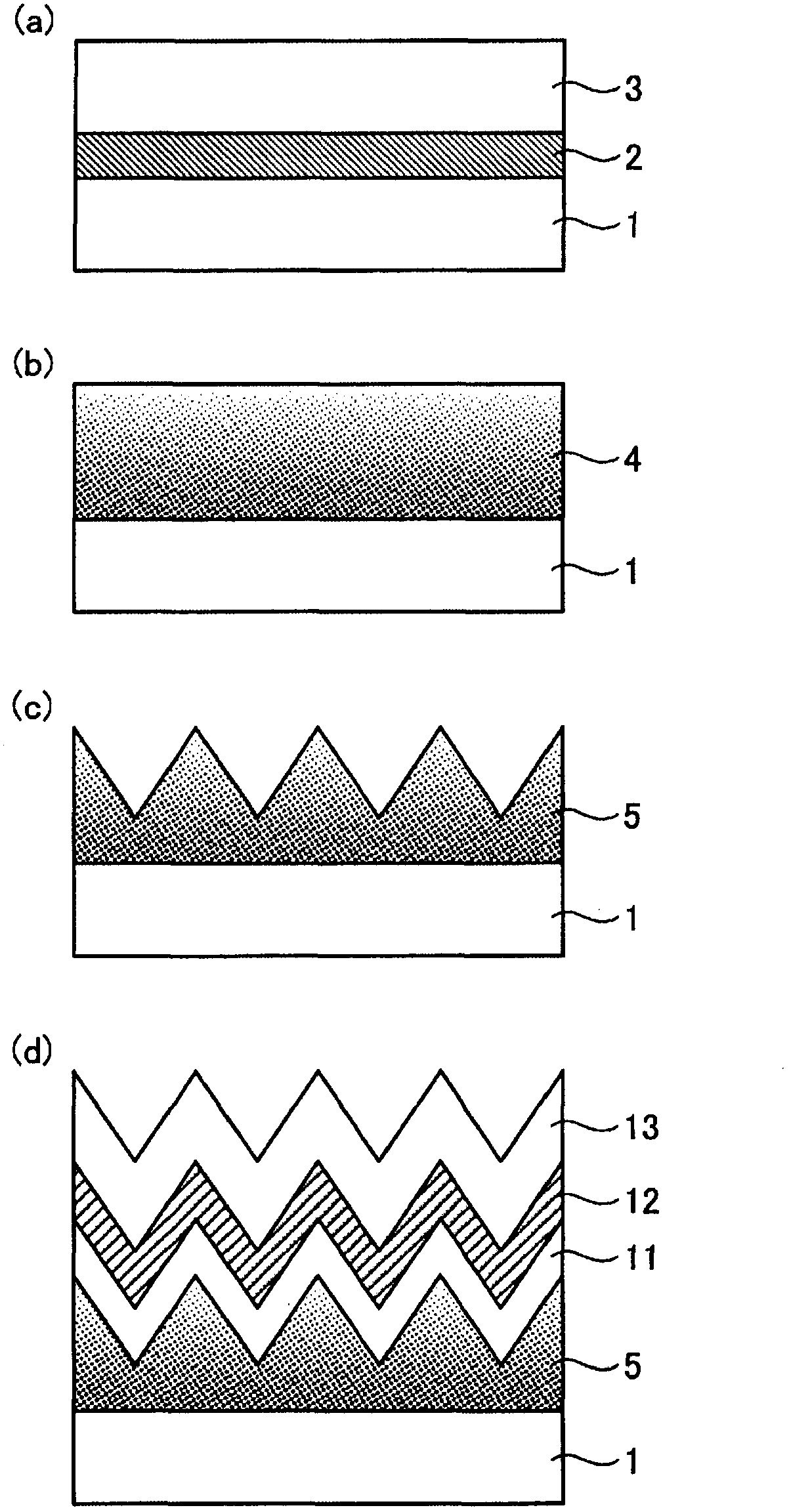
[0024] figure 1 It is a cross-sectional view schematically showing a method of manufacturing a transparent electrode and a method of manufacturing a photoelectric conversion device according to Embodiment 1 of the present invention. Here, an aluminum (Al) thin film will be described as an example of a dopant-containing thin film composed of a dopant-containing material. First, if figure 1 As shown in (a), an aluminum thin film 2 and a zinc oxide (ZnO)-based thin film 3 are sequentially stacked on a light-transmitting insulating substrate 1 . As the translucent insulating substrate 1 , various translucent insulating substrates such as glass, transparent resin, plastic, and quartz are used.

[0025] For the zinc oxide-based thin film 3 , for example, a zinc oxide film is used. Zinc oxide is one of transparent conductive oxides (TCO: Transparent Conductive Oxide) generally used as a transparent electrode material. Furthermore, the zinc oxide-based thin film 3 has zinc oxide a...

Embodiment approach 2

[0052] Image 6 It is a cross-sectional view schematically showing a method of manufacturing a transparent electrode and a method of manufacturing a photoelectric conversion device according to Embodiment 2 of the present invention. The manufacturing method of the transparent electrode of Embodiment 2 is different from the manufacturing method of the transparent electrode of Embodiment 1 in that the etching step is performed both before and after the thermal diffusion step. Hereinafter, the same symbols are assigned to the same components as in Embodiment 1. FIG.

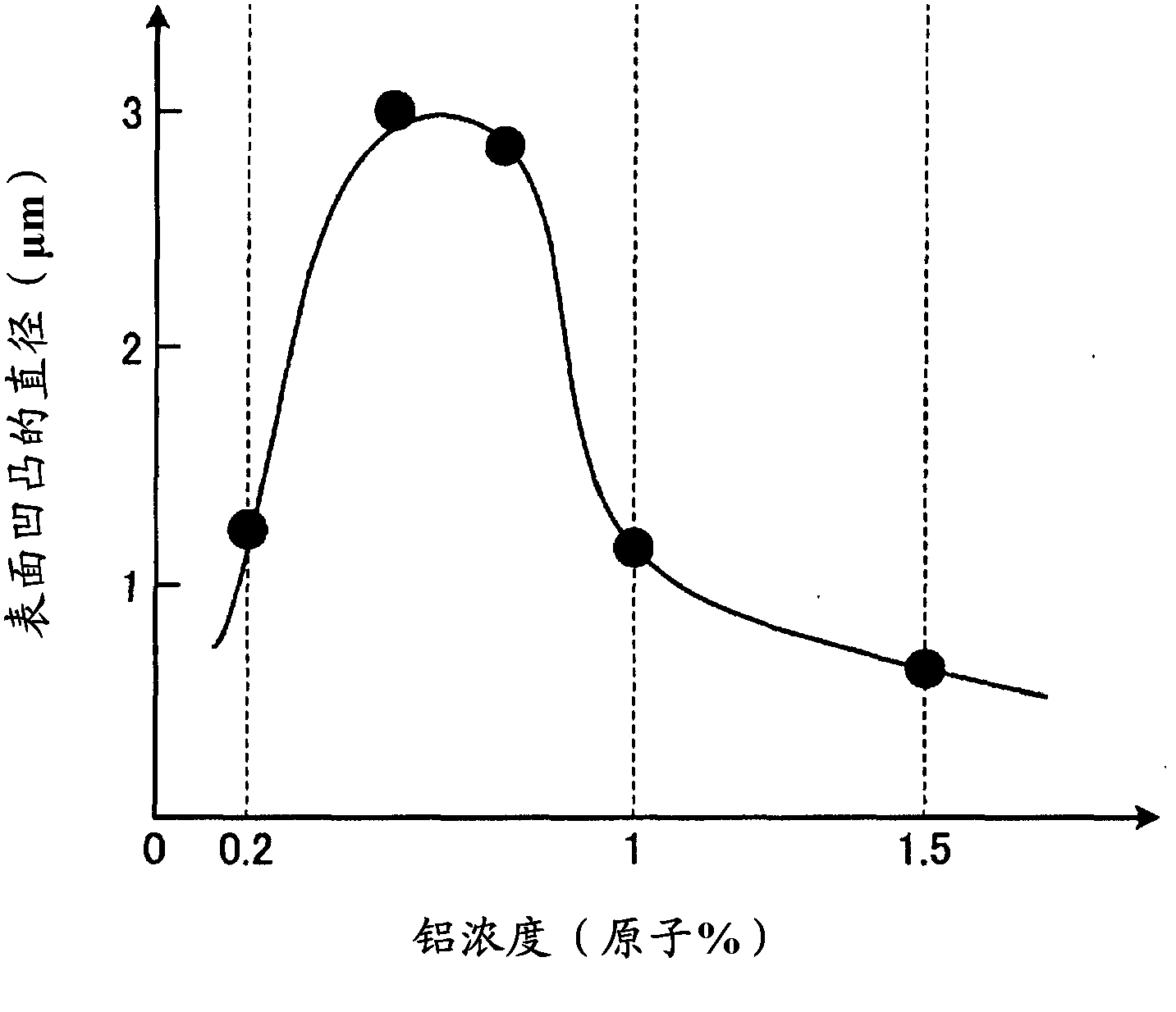
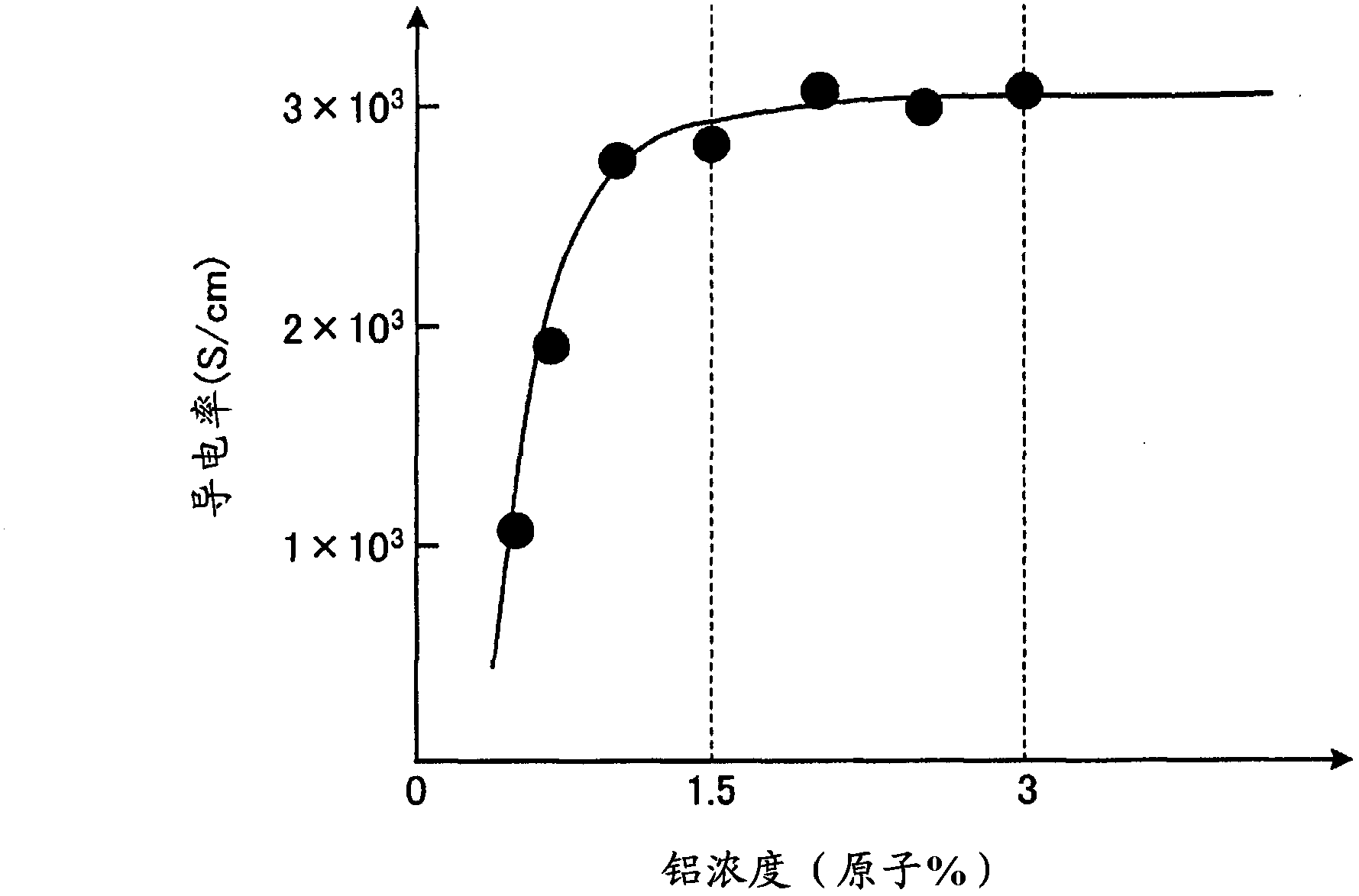
[0053] It has been reported that the shape of the surface irregularities formed on the surface of the zinc oxide thin film by etching is based on figure 2 The aluminum concentration in the zinc oxide-based thin film shown, and the temperature at the time of film formation of the zinc oxide-based thin film, and the thermal history of the film such as heat treatment vary. In Embodiment 2, a higher light-scattering ...

Embodiment approach 3

[0072] Figure 7 It is a cross-sectional view schematically showing a method of manufacturing a transparent electrode and a method of manufacturing a photoelectric conversion device according to Embodiment 3 of the present invention. The method for manufacturing a transparent electrode according to Embodiment 3 differs from the method for manufacturing a transparent electrode according to Embodiment 1 in that an etching step is omitted by using MOCVD in forming the zinc oxide-based thin film. Hereinafter, the same reference numerals are attached to the same components as in the first embodiment.

[0073] First, if Figure 7As shown in (a), after an aluminum thin film 2 is formed on a light-transmitting insulating substrate 1 , a zinc oxide-based thin film 6 having surface irregularities is stacked by MOCVD. Furthermore, the translucent insulating substrate 1, the aluminum thin film 2, and the zinc oxide-based thin film 6 can be selected from various materials described in th...


PUM

PropertyMeasurementUnit
thicknessaaaaaaaaaa
thicknessaaaaaaaaaa
thicknessaaaaaaaaaa

Abstract

A transparent electrode substrate in which a transparent electrode formed from a zinc oxide-based thin film is formed on a translucent insulating substrate, the zinc oxide-based thin film containing zinc oxide as the main component and at least one type of dopant element. The zinc oxide-based thin film has an uneven surface and a dopant element concentration gradient in which the concentration of the dopant element continuously decreases from the side of the translucent insulating substrate to the surface of the zinc oxide-based thin film. The concentration of the dopant element in the zinc oxide-based thin film is 1.5 atom % to 3 atom % in a region from the translucent insulating substrate to 50 nm inward in the thickness direction and is 0.2 atom % to 1 atom % in a region from the surface of the zinc oxide-based thin film to 300 nm inward in the thickness direction.

Description

technical field [0001] The invention relates to a transparent electrode substrate and a manufacturing method thereof, a photoelectric conversion device and a manufacturing method thereof, and a photoelectric conversion module. Background technique [0002] In a photoelectric conversion device, a transparent electrode is one of important factors. High light transmittance and conductivity are required for transparent electrodes. Mainly, the light transmittance has an influence on the short-circuit current density (Jsc), and the conductivity has an influence on the fill factor (FF). In particular, when only the transparent electrode is used as the electrode on the light-receiving side, the current generated in the photoelectric conversion layer has a lateral current path, so it is important to improve the conductivity. In addition, it is known that by providing irregularities on the surface of the transparent electrode to scatter light and lengthen the optical path, Jsc is in...

Claims


Application Information

Patent Timeline
Patent Type & Authority Applications(China)
IPC IPC(8): H01B5/14H01B13/00H01L31/04
CPCH01L31/022483H01L31/02366Y02E10/50
Inventor 菅原胜俊小西博文山林弘也
Owner MITSUBISHI ELECTRIC CORP
Why Eureka
Try Eureka