Semiconductor laser device

A technology of lasers and semiconductors, applied in semiconductor laser devices, semiconductor lasers, laser devices, etc., can solve problems such as inability to fully satisfy temperature characteristics, high polarization ratio, etc., and achieve improved photoelectric conversion efficiency, high polarization ratio, and improved heat release Effect

Active Publication Date: 2009-12-09
PANASONIC SEMICON SOLUTIONS CO LTD
View PDF3 Cites 8 Cited by
  • Summary
  • Abstract
  • Description
  • Claims
  • Application Information

AI Technical Summary

Problems solved by technology

[0020] Therefore, just to make the effective refractive index difference (ΔN) 3×10 -3 ~7×10 -3 However, simply forming a groove between the wing area and the ridge cannot fully satisfy good temperature characteristics, high polarization ratio, FFP without disturbance, and high kink light output.

Method used


Image

  • Semiconductor laser device
  • Semiconductor laser device
  • Semiconductor laser device

Examples


no. 1 Embodiment approach

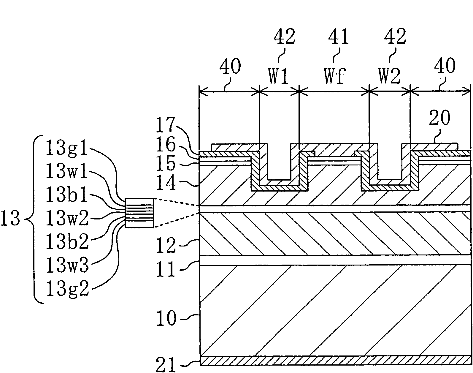
[0124] figure 1 The cross-sectional structure of the semiconductor laser device according to the first embodiment of the present invention is shown.

[0125] In this configuration, a red laser and an infrared laser are integrated on an n-type GaAs substrate 10 whose main surface is a surface inclined at 10° from the (100) plane to the [011] direction. First, explain figure 1 Construction of the red laser shown.

[0126] The red laser is formed with n-type GaAs buffer layer 11 (0.5 μm), n-type (Al 0.7 Ga 0.3 ) 0.51 In 0.49 P cladding layer 12 (2.0μm), distorted quantum well active layer 13, p-type (Al 0.7 Ga 0.3 ) 0.51 In 0.49 P cladding layer 14, p-type Ga 0.51 In 0.49 P protective layer 15 p-type GaAs contact layer (0.4 μm) 16 . Distorted quantum well active layer 13 is as shown in the figure (Al 0.5 Ga 0.5 ) 0.51 In 0.49 A stacked structure of P first guide layer 13g1, GaInP well layer 13w1-w3, AlGaInP barrier layers 13b1, 13b2, and AlGaInP second guide l...

no. 2 Embodiment approach

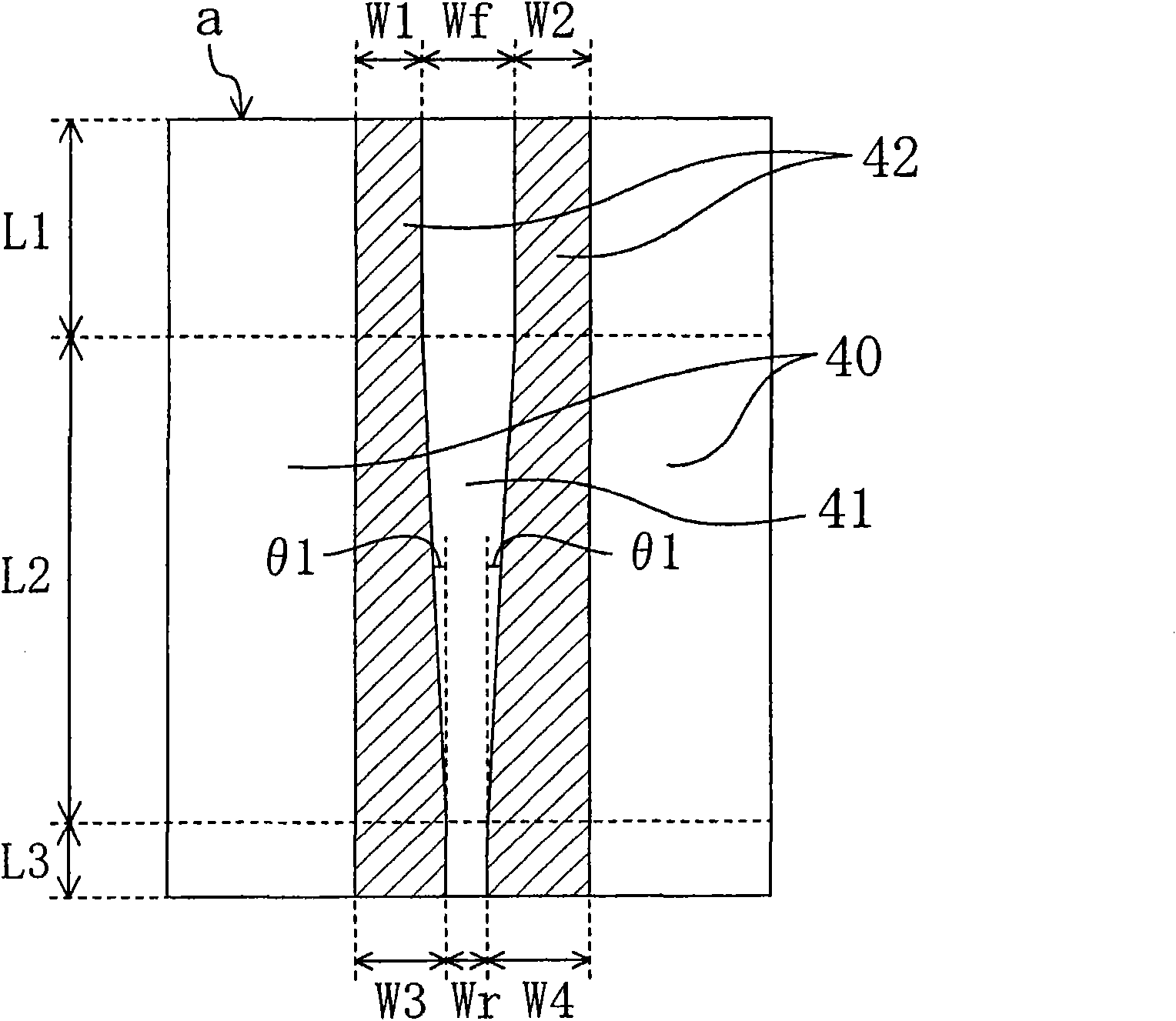
[0153] Figure 9 The ridge shape and the wing region shape of the semiconductor laser device according to the second embodiment of the present invention are shown. In addition, the shape of the ridge 41 is the same as the structure of the ridge 41 described in the first embodiment of the present invention (refer to figure 2 ).

[0154] Figure 9 The wing region 40 shown increases the width of the groove 42 within the region of the tapered shape where the ridge width decreases with respect to the resonator direction, so that the distance between the central portion of the ridge 41 and the wing region 40 increases. When the shape of the ridge 41 is tapered, the propagating light of the waveguide leaks from the sidewall of the ridge 41 , and the scattered light diffuses into the wing region 40 . When the scattered light reaches the wing region 40, there is a difference in effective refractive index between the wing region 40 and the groove 42, so it is reflected at the interf...

Deformed example 1-

[0161] Figure 11 The ridge shape and the shape of the wing region in Modification 1 of the semiconductor laser device according to the second embodiment of the present invention are shown. In addition, the shape of the ridge 41 is the same as the structure of the ridge 41 described in the first embodiment of the present invention (refer to figure 2 ).

[0162] Figure 11 The wing region 40 is shown increasing in width from the front end to the rear end face of the groove 42 so that the distance between the central portion of the ridge 41 and the wing region 40 increases.

[0163] Such a structure can also prevent a decrease in kink light output. In Modification 1, the widths W1 and W2 are set to 6 μm, and the widths W3 and W4 are set to 11 μm in order to improve the kink light output and realize FFP without disturbance.


PUM


Abstract

The invention provides a semiconductor laser device with good temperature characteristic, high polarization rate and high refraction light output. A semiconductor laser device includes an n-type clad layer, an active layer, and a p-type clad layer having a ridge and wing regions. The wing regions are provided with a first trench present on one side of the ridge and a second trench provided on the other side thereof being interposed therebetween. A reflectivity Rf at a front end face of a resonator, a reflectivity Rr at a rear end face of the resonator, a minimum value W1 of a width of the first trench in a region adjacent to the front end face, a minimum value W2 of a width of the second trench in the region adjacent to the front end face, a width W3 of the first trench at the rear end face, and a width W4 of the second trench at the rear end face satisfy Rf<Rr, W1<W3, and W2<W4. A width Wf of the ridge at the front end face, and a width Wr of the ridge at the rear end face satisfy Wf>Wr. The ridge includes a region where a width decreases with distance from the front end side toward the rear end side.

Description

technical field [0001] The present invention relates to a semiconductor laser device having a high thermally saturated optical output and a low operating current in a high-temperature high-output operating state. Background technique [0002] Semiconductor laser devices (hereinafter also referred to as semiconductor lasers) are widely used in various fields. For example, AlGaInP series semiconductor lasers are widely used as light sources in the field of optical disk systems represented by DVD because they can obtain red laser light with a wavelength of 650 nm. Among semiconductor lasers, there are known lasers in which a dielectric film is used for the current block layer in the manufacturing process of the semiconductor laser in order to reduce the manufacturing cost and shorten the lead time, so as to reduce the number of times of crystal growth (for example, refer to Patent Document 1). [0003] Figure 21 An example of an AlGaInP series semiconductor laser having such...

Claims


Application Information

Patent Timeline
Patent Type & Authority Applications(China)
IPC IPC(8): H01S5/343H01S5/028H01S5/22H01S5/24H01S5/10H01S5/40
CPCH01S5/4087H01S2301/14H01S5/4031H01S5/34326H01S5/1064H01S5/34313H01S5/22B82Y20/00
Inventor 高山彻早川功一佐藤智也佐佐木正隼木户口勋
Owner PANASONIC SEMICON SOLUTIONS CO LTD
Why Eureka
Try Eureka